PCB Design Checklist Before Manufacturing
Reduce Manufacturing Risk. Improve Product Reliability. Release Every PCB with Confidence.
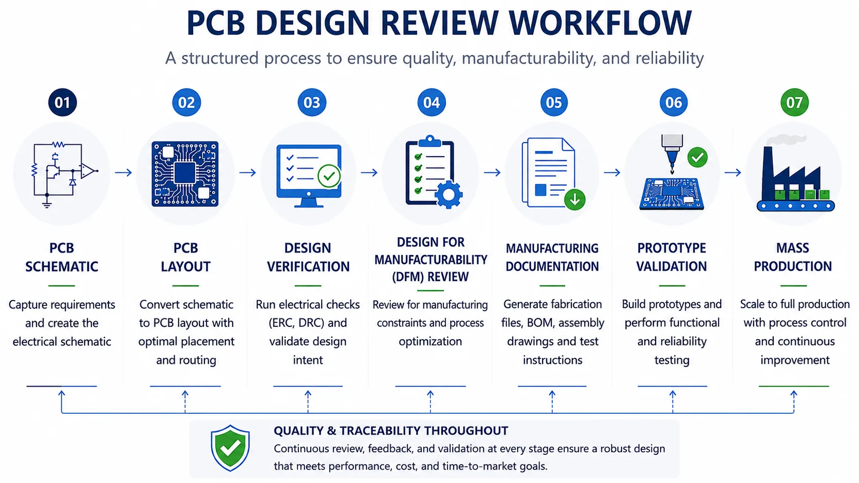
A structured engineering review significantly reduces manufacturing defects and prevents costly redesign cycles later in production.
Whether you're designing your first prototype or preparing a complex multilayer PCB for mass production, a structured design review before manufacturing can prevent costly fabrication errors, assembly issues, schedule delays, and unnecessary redesigns.
This guide presents a practical engineering checklist based on proven Design for Manufacturability (DFM) principles used across the electronics manufacturing industry. Rather than focusing solely on CAD design rules, it explains how experienced manufacturing engineers evaluate PCB designs before they reach the factory floor.
By the end of this guide, you'll understand not only what to verify, but why each design decision influences fabrication, assembly, testing, product reliability, and manufacturing cost.
1. Executive Summary
Every PCB design eventually reaches the same critical milestone: the transition from engineering design to manufacturing.
Surprisingly, this transition is where many avoidable problems originate.
A PCB may pass every electrical design rule check (DRC) within the CAD software and still encounter fabrication challenges, assembly delays, unexpected yield losses, or product reliability issues during manufacturing. These problems often arise because successful PCB production depends on far more than electrical connectivity. Mechanical constraints, manufacturing tolerances, assembly processes, material selection, documentation quality, component availability, and testing strategy all play equally important roles.
Manufacturing engineers frequently encounter preventable issues such as:
•
Copper traces placed too close to routed board edges
•
Missing fiducial marks for automated assembly
•
Inadequate solder mask clearance
•
Poor thermal management for power components
•
Incorrect drill-to-pad relationships
•
Ambiguous fabrication drawings
•
Missing assembly documentation
•
Components placed too close together for automated inspection or rework
•
PCB stack-ups that exceed the manufacturer's process capability
While each issue may appear minor during layout, their cumulative effect can lead to increased manufacturing costs, delayed product launches, lower production yields, and reduced long-term product reliability.
This guide provides a structured engineering checklist that bridges the gap between PCB design and successful manufacturing. Drawing upon industry best practices and relevant IPC guidance, it explains the reasoning behind each review stage while offering practical recommendations that can be incorporated into everyday design workflows.
Rather than treating Design for Manufacturability (DFM) as a final verification step, this guide encourages engineers to integrate manufacturing considerations throughout the design process. Doing so reduces design iterations, shortens time-to-market, improves production consistency, and strengthens collaboration between design teams and manufacturing partners.
2. Introduction
Modern electronic products are expected to deliver higher performance, greater reliability, smaller form factors, and lower production costs than ever before. At the same time, product development schedules continue to shrink while design complexity steadily increases.
Printed Circuit Boards (PCBs) now routinely incorporate:
•
High-speed digital interfaces
•
Dense component placement
•
Fine-pitch packages
•
Mixed-signal circuits
•
RF modules
•
High-current power electronics
•
Multiple voltage domains
•
Thermal management requirements
•
Electromagnetic compatibility (EMC) considerations
Designing such systems requires balancing electrical performance, mechanical integrity, manufacturability, serviceability, cost, and long-term reliability.
Unfortunately, many PCB reviews still focus almost exclusively on schematic correctness and CAD rule compliance.
This approach overlooks an important reality:
A PCB is not successful simply because it can be manufactured. It is successful when it can be manufactured consistently, assembled efficiently, tested reliably, and operated safely throughout its intended service life.
That distinction forms the foundation of modern Design for Manufacturability (DFM).
DFM is not a checklist performed after layout is complete. It is an engineering philosophy that influences decisions from component selection and stack-up planning through routing, documentation, assembly, testing, and production release.
Organizations that integrate manufacturing considerations early often experience:
•
Higher first-pass manufacturing yield
•
Reduced engineering change orders (ECOs)
•
Faster new product introduction (NPI)
•
Lower production costs
•
Fewer field failures
•
Improved supplier collaboration
•
Greater schedule predictability
Conversely, overlooking manufacturability during design can result in repeated prototype iterations, production delays, increased scrap rates, and expensive redesign efforts that could have been avoided through a systematic engineering review.
This guide aims to provide that systematic review framework.
3. Engineering Insight
Passing Design Rule Checks (DRC) does not guarantee manufacturability. DRC verifies compliance with predefined CAD rules, whereas Design for Manufacturability evaluates whether the PCB can be fabricated, assembled, inspected, tested, and produced consistently within real manufacturing constraints.
4. Why PCB Designs Fail During Manufacturing
One of the most common misconceptions among new hardware teams is that manufacturing failures originate primarily from fabrication defects.
In reality, a significant proportion of manufacturing issues can be traced back to design decisions made long before the PCB reaches the production floor.
These issues typically fall into several categories:
Design Stage | Common Oversight | Manufacturing Impact |
|---|---|---|
Mechanical Design | Incorrect board outline or mounting holes | Assembly interference and enclosure fit issues |
PCB Layout | Inadequate trace spacing or copper clearance | Fabrication defects and reduced yield |
Component Placement | Insufficient spacing between components | Difficult assembly, soldering and inspection |
Thermal Design | Poor heat dissipation | Component overheating and reduced reliability |
Documentation | Missing fabrication or assembly notes | Manufacturing delays and engineering queries |
Supply Chain | Obsolete or unavailable components | Procurement delays and redesign |
5. Manufacturing Perspective
Manufacturers rarely reject a PCB because it is electrically incorrect. More often, they identify issues that make the board difficult, inconsistent, or unnecessarily expensive to manufacture. A design that anticipates manufacturing realities typically progresses through production with fewer questions, fewer delays, and higher yields.
6. Engineering Review Checklist
6.1. Define Product Requirements Before Opening Your PCB CAD Tool
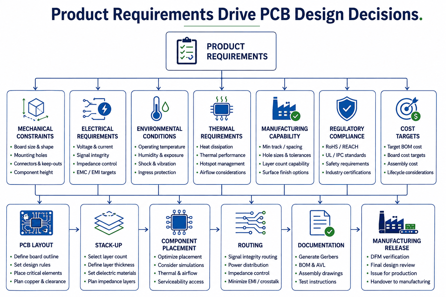
Many PCB design problems originate long before the first component is placed on the board.
A common mistake among development teams is beginning PCB layout immediately after completing the schematic. While the schematic defines electrical functionality, it does not capture the mechanical, manufacturing, environmental, or commercial constraints that ultimately determine whether the product can be manufactured reliably and economically.
Experienced hardware teams therefore begin every PCB project with a clear definition of product requirements before starting the physical layout.
This initial planning stage influences almost every downstream engineering decision, including PCB dimensions, layer count, stack-up, material selection, component placement strategy, thermal management, manufacturability, assembly complexity, and overall production cost.
Skipping this step often results in repeated PCB revisions, schedule delays, and unnecessary engineering effort.
Engineering Checklist
Before beginning PCB layout, confirm that the following questions have been answered:
✓ What is the intended application of the PCB?
✓ Is this a prototype, pilot build, or mass-production design?
✓ What environmental conditions will the product experience?
✓ What operating temperature range is required?
✓ Are vibration or shock requirements applicable?
✓ What reliability or expected service life is required?
✓ What certifications or regulatory requirements must be satisfied?
✓ What is the target manufacturing quantity?
✓ Which PCB manufacturer capabilities will be used?
✓ What cost targets must be achieved?
Engineering Insight
PCB layout is an engineering optimization exercise, not simply a drawing activity. Every design decision should balance electrical performance, manufacturability, reliability, serviceability, and cost simultaneously.
6.2 Define the Board Outline and Mechanical Constraints
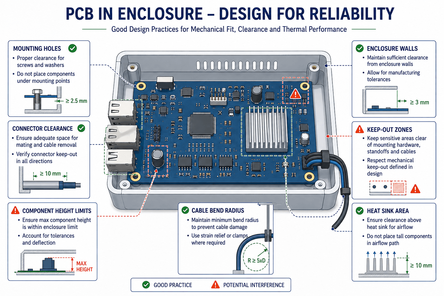
The mechanical definition of a PCB is frequently underestimated during early design stages. Yet mechanical errors remain one of the leading causes of late-stage redesigns because they often become apparent only after prototype assembly.
Before placing a single component, the board outline should already be considered frozen or subject to formal mechanical change control.
Mechanical design encompasses significantly more than the outer dimensions of the PCB. It defines how the board interfaces with the enclosure, connectors, mounting hardware, heat sinks, displays, batteries, wiring harnesses, and neighboring assemblies.
Poor mechanical planning frequently results in:
•
Connectors that cannot be accessed after assembly.
•
Components colliding with enclosure walls.
•
Mounting holes interfering with copper pours.
•
Tall components conflicting with adjacent assemblies.
•
Insufficient clearance around screws or standoffs.
•
Inadequate keep-out zones.
Correcting these issues after routing is substantially more expensive than identifying them before layout begins.
Mechanical Design Review Checklist
Review the following items before starting PCB placement:
Item | Review Questions |
|---|---|
PCB Dimensions | Does the PCB fit the enclosure with sufficient manufacturing tolerance? |
Mounting Holes | Are hole locations mechanically verified? |
Connector Access | Can cables be connected after assembly? |
Height Restrictions | Do component heights satisfy enclosure limits? |
Keep-Out Areas | Are mechanical keep-out zones defined? |
Heat Sink Space | Is sufficient space available for cooling hardware? |
Test Access | Can production test fixtures reach required locations? |
Manufacturing Perspective
Manufacturing engineers often discover enclosure interference only after prototype assembly. At that stage, even a few millimetres of dimensional error may require redesigning the PCB, enclosure, or both. Mechanical verification before layout is one of the least expensive engineering reviews you can perform.
Engineering Case Study
Connector Placement Caused Full PCB Redesign
An industrial communication gateway was designed with two RJ45 connectors positioned close to the enclosure wall.
The PCB passed all electrical verification and prototype assembly.
However, during final mechanical integration, the Ethernet cables could not be inserted because the connector latches collided with the enclosure housing.
Although the PCB itself functioned correctly, the entire layout required redesign, delaying product launch by three weeks.
Engineering Lesson
Mechanical fit should always be validated using the complete product assembly—not only the PCB CAD model.
IPC Standard Reference
IPC-2221 – Generic Standard on Printed Board Design
IPC-2221 establishes widely accepted design practices covering conductor spacing, mechanical design considerations, hole dimensions, creepage distances, and general PCB layout recommendations.
While manufacturers may support tighter process capabilities than the minimum values defined by IPC-2221, using the standard as a baseline promotes designs that are compatible with a broad range of fabrication processes and manufacturing suppliers.
Practical Guidance
Treat IPC-2221 as your starting point rather than your design limit. Always confirm whether your manufacturing partner offers process capabilities beyond the standard before reducing clearances or tolerances.
6.3 Select the Appropriate PCB Material
One of the most overlooked design decisions is choosing PCB material based solely on habit or cost.
FR-4 is often selected by default because it satisfies the needs of many commercial electronics products. However, PCB material influences electrical performance, thermal behaviour, moisture resistance, dimensional stability, and manufacturing reliability.
Material selection should therefore reflect the intended application rather than follow a one-size-fits-all approach.
Factors that influence PCB material selection include:
•
Operating frequency
•
Maximum operating temperature
•
Thermal cycling requirements
•
Power dissipation
•
Environmental exposure
•
Mechanical stress
•
Product lifespan
•
Regulatory requirements
•
Manufacturing process compatibility
Selecting an inappropriate material can introduce reliability issues that may not become apparent until the product has been deployed in the field.
Engineering Insight
Material selection is not simply a purchasing decision. It is an engineering decision that affects electrical performance, thermal management, long-term reliability, manufacturability, and overall product lifecycle cost.
6.4 Plan the PCB Stack-up Before Routing
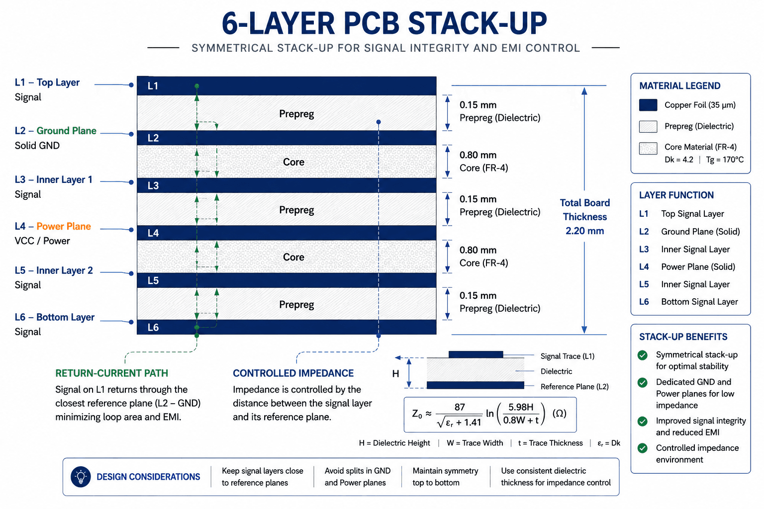
The PCB stack-up is the structural foundation of every printed circuit board. It defines how copper layers, dielectric materials, and reference planes are arranged within the board. Once routing begins, changing the stack-up often requires significant redesign effort, making early planning essential.
Many first-time designers treat the stack-up as a decision to make after routing has started. Experienced engineers take the opposite approach—they establish the stack-up before placing components because it directly influences signal integrity, power distribution, impedance control, electromagnetic compatibility (EMC), thermal behaviour, manufacturability, and overall production cost.
An inappropriate stack-up can introduce problems that are difficult or impossible to correct later, including poor return-current paths, impedance variations, excessive EMI, unnecessary board thickness, and increased fabrication costs.
Why Stack-up Planning Matters
A well-designed stack-up provides:
•
Continuous reference planes for signal return paths
•
Controlled impedance for high-speed interfaces
•
Reduced electromagnetic emissions
•
Improved power distribution
•
Better isolation between noisy and sensitive circuits
•
Greater mechanical rigidity
•
More predictable manufacturing outcomes
Conversely, a poorly planned stack-up often leads to signal integrity issues that cannot be solved by routing changes alone.
Engineering Checklist – Stack-up Planning
Before routing begins, verify the following:
Review Item | Engineering Question |
|---|---|
Layer Count | Is the selected layer count sufficient for routing density and signal integrity? |
Ground Plane | Is there at least one uninterrupted ground reference plane? |
Power Plane | Are power planes sized appropriately for current demand? |
High-Speed Signals | Can critical traces reference a continuous return plane? |
Controlled Impedance | Has impedance been calculated using the manufacturer's stack-up? |
Copper Balance | Is copper distributed evenly to minimise board warpage? |
Board Thickness | Does the total thickness satisfy connector and enclosure requirements? |
Engineering Insight
Choosing a six-layer board instead of forcing everything onto four layers can often reduce overall project cost. Although fabrication costs increase slightly, routing becomes simpler, EMI performance improves, prototype iterations decrease, and engineering time is significantly reduced.
Manufacturing Perspective
PCB manufacturers define specific dielectric materials, prepreg thicknesses, copper weights, and process tolerances.
Designing an arbitrary stack-up without consulting the intended manufacturer frequently results in stack-up revisions before fabrication can begin.
Whenever possible, request the manufacturer's recommended stack-up for your chosen board thickness and layer count before finalising the layout.
This simple step eliminates many unnecessary engineering questions during fabrication review.
Engineering Case Study
Four Layers Were Not Enough
A startup developing an industrial IoT controller attempted to route high-speed Ethernet, USB, isolated power supplies, and multiple sensor interfaces on a four-layer PCB to reduce manufacturing cost.
The design eventually required:
•
Excessive vias
•
Split ground planes
•
Long routing paths
•
Multiple signal crossovers
Signal integrity issues appeared during prototype testing, followed by EMC failures during compliance evaluation.
The board was redesigned using a six-layer stack-up.
The manufacturing cost increased by approximately 12%, but:
•
Routing complexity decreased dramatically
•
EMC compliance was achieved
•
Engineering redesign time was eliminated
•
Overall project cost was lower because an additional prototype spin was avoided
Engineering Lesson
Optimising only fabrication cost can increase total product development cost.
A PCB should be optimised for the entire product lifecycle—not just the board price.
6.5 Select Appropriate Copper Weight and Trace Width
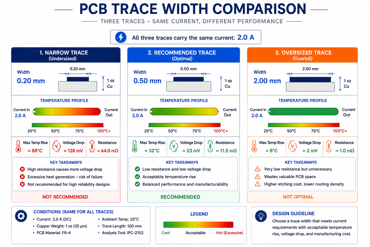
Copper traces are the electrical highways of a PCB. Selecting an appropriate trace width involves far more than fitting traces between component pads.
Trace dimensions influence:
•
Current carrying capacity
•
Temperature rise
•
Voltage drop
•
Manufacturing yield
•
Reliability
•
Long-term product performance
Designers sometimes reduce trace widths to simplify routing without evaluating electrical consequences. While modern fabrication processes can produce extremely fine traces, unnecessarily narrow conductors increase resistance, generate more heat, and reduce manufacturing margin.
Conversely, excessively wide traces may create routing congestion and increase PCB size.
The objective is to select trace widths that satisfy both electrical and manufacturing requirements.
Engineering Checklist – Copper and Routing
Verify the following:
✓ Trace widths are calculated for expected operating current.
✓ Copper weight is appropriate for power distribution.
✓ High-current paths have sufficient width.
✓ Thermal rise has been evaluated.
✓ Voltage drop is acceptable.
✓ Manufacturing minimum trace/space rules are satisfied.
✓ Fine-pitch components are compatible with selected fabrication capability.
Engineering Insight
Do not design to the absolute minimum trace width advertised by a PCB manufacturer simply because it is possible. Designing with reasonable manufacturing margins generally improves fabrication yield and reduces production variability.
IPC Standard Reference
IPC-2221 – Conductor Width Guidance
IPC-2221 provides engineering guidance for selecting conductor widths based on:
•
Current
•
Temperature rise
•
Copper thickness
•
External versus internal layers
Modern PCB CAD tools include trace width calculators, but engineers should always validate assumptions against the manufacturer's recommended design rules.
6.6 Design Continuous Return Current Paths
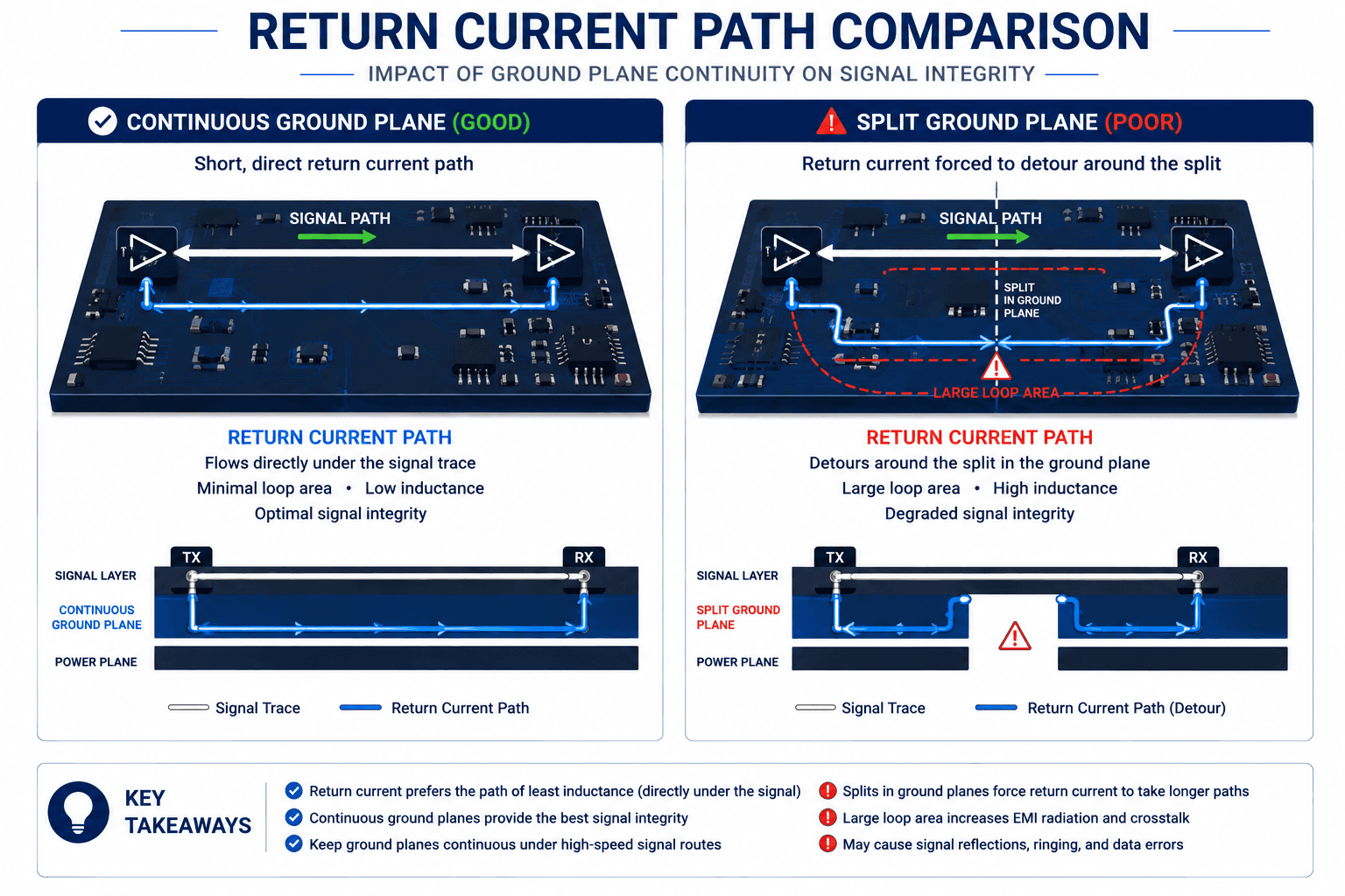
One of the most misunderstood concepts in PCB design is return current.
Many engineers assume electrical current simply follows the shortest physical route back to its source.
In reality, alternating current—and especially high-speed digital signals—returns along the path of lowest impedance, which is typically the continuous reference plane directly beneath the signal trace.
Interrupting that reference plane with splits, slots, or gaps forces return currents to detour around the obstacle. This increases loop area, resulting in:
•
Higher electromagnetic emissions
•
Increased susceptibility to external noise
•
Crosstalk
•
Signal distortion
•
Reduced signal integrity
Maintaining uninterrupted reference planes is therefore one of the most effective methods of improving PCB performance without adding cost.
Engineering Insight
Every signal forms a complete circuit. When routing high-speed signals, design the return-current path with the same attention given to the signal trace itself.
Manufacturing Perspective
Although return-current design primarily affects electrical performance rather than fabrication, poor reference plane planning often leads to additional PCB revisions after prototype validation. These redesigns delay product introduction and increase overall development cost.
6.7 Plan Component Placement Before Routing
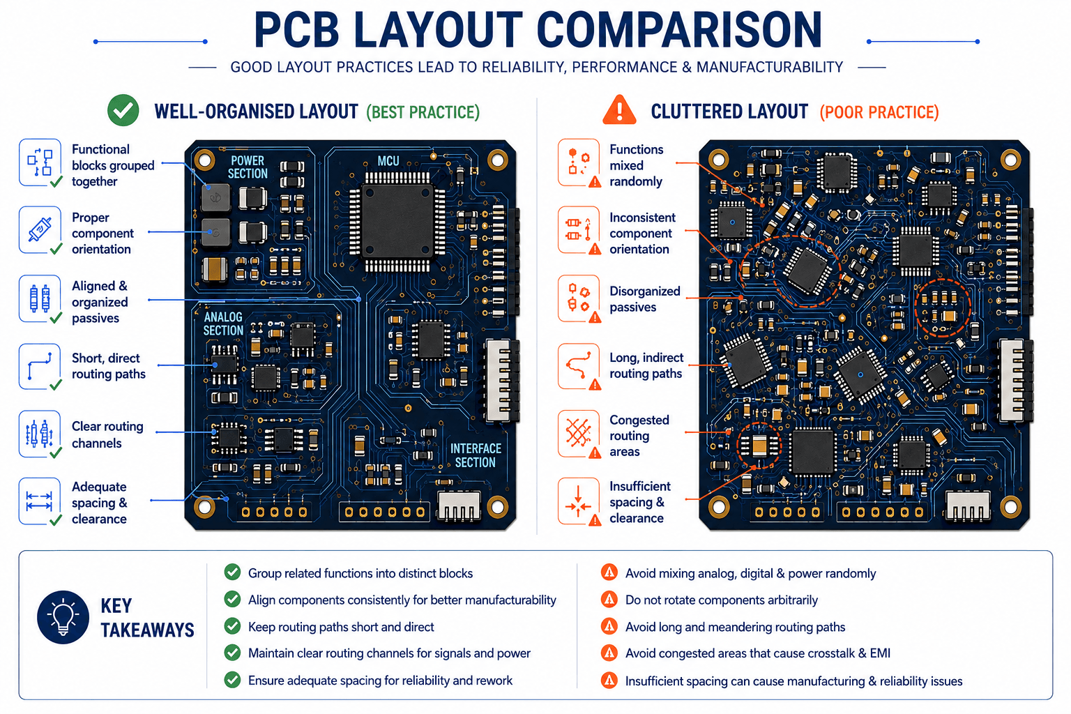
Ask experienced PCB designers about the secret to a clean layout, and many will tell you the same thing:
Good routing begins with good component placement.
Once traces are routed, moving even a single major component can trigger a cascade of changes across the PCB. For this reason, experienced engineers spend a significant portion of the layout phase refining component placement before routing begins.
Component placement is far more than arranging parts to fit within the board outline. It determines electrical performance, thermal behaviour, manufacturability, testability, serviceability, and assembly efficiency.
A well-organised layout naturally produces shorter traces, fewer vias, cleaner power distribution, and improved signal integrity. Poor placement often forces compromises that no amount of routing optimisation can completely overcome.
Practical Placement Strategy
A systematic placement workflow generally follows this order:
•
Place mechanically constrained components (connectors, switches, displays, mounting holes).
•
Position large components such as transformers, inductors, and heatsinks.
•
Group related circuitry into functional blocks.
•
Place high-speed devices close to their associated memory or interfaces.
•
Position power conversion circuits together.
•
Place passive components around their associated ICs.
•
Leave routing channels before filling remaining board space.
This approach simplifies routing while improving readability for future maintenance and design reviews.
Engineering Checklist – Component Placement
Before routing begins, verify:
✓ Connectors align correctly with the enclosure.
✓ High-speed ICs are located close to associated devices.
✓ Analogue and digital circuits are physically separated where appropriate.
✓ High-current paths are short and direct.
✓ Heat-generating components are not clustered unnecessarily.
✓ Sensitive analogue circuits are isolated from switching regulators.
✓ Test points remain accessible.
✓ Rework clearance exists around large ICs.
✓ Polarised components are oriented consistently.
✓ Reference designators remain visible after assembly where practical.
Engineering Insight
A PCB should tell a story. When an experienced engineer looks at the layout, they should immediately recognise power sections, analogue blocks, digital processing, communication interfaces, and connectors without referring to the schematic.
Manufacturing Perspective
Automated assembly machines perform best when components are placed with adequate spacing, consistent orientation, and sufficient access for optical inspection.
A layout that is electrically correct but difficult to inspect or rework often increases manufacturing cost far more than designers expect.
Engineering Case Study
Dense Placement Increased Assembly Defects
A consumer electronics manufacturer reduced PCB size by placing numerous passive components immediately adjacent to a fine-pitch microcontroller.
Prototype assembly succeeded.
However, during volume production:
•
AOI inspection produced frequent false calls.
•
Manual rework became difficult.
•
Several solder bridges required operator intervention.
•
Assembly throughput decreased significantly.
A modest increase in PCB area allowed improved spacing, reducing assembly defects and shortening production time.
Engineering Lesson
Board area is not always the most expensive resource. In many cases, additional PCB space reduces manufacturing cost by simplifying assembly and inspection.
6.8 Place Decoupling Capacitors Correctly
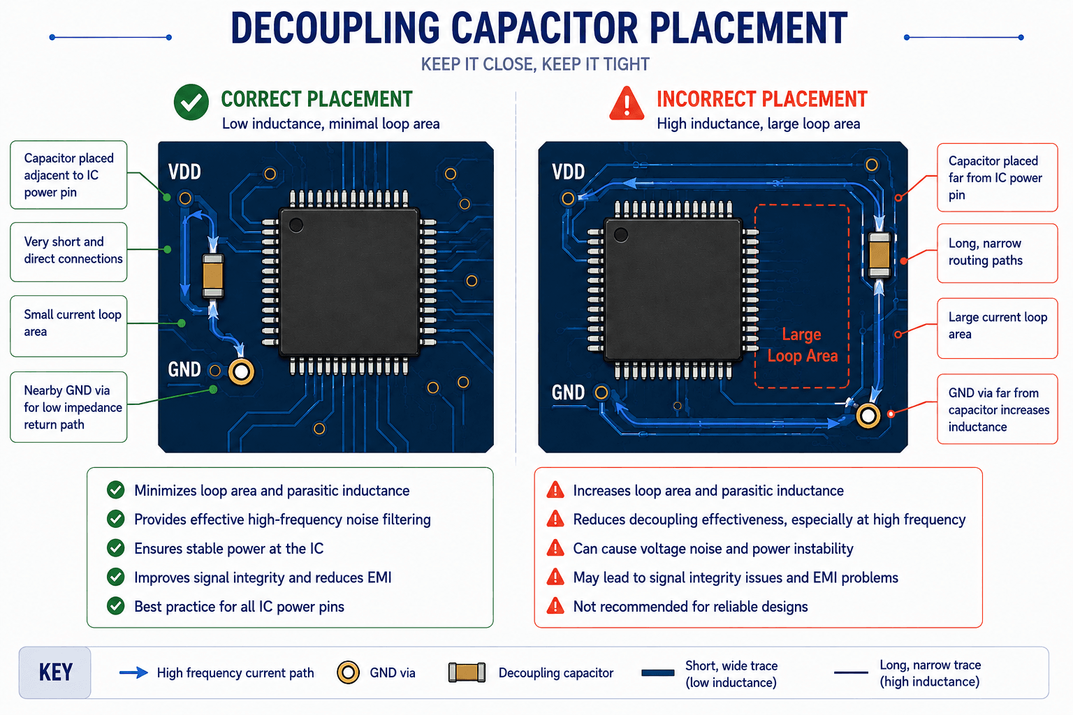
Decoupling capacitors are among the smallest components on a PCB, yet they play one of the largest roles in maintaining power integrity.
Every integrated circuit draws rapidly changing currents during operation. Without nearby energy storage, these transient demands create voltage fluctuations that may lead to unstable operation, increased electromagnetic emissions, or intermittent system failures.
A capacitor placed only a few centimetres away may appear electrically connected on the schematic, yet perform poorly because of the additional inductance introduced by longer PCB traces.
Successful decoupling depends on physical placement, not simply electrical connectivity.
Best Practices
•
Place decoupling capacitors on the same side of the PCB as the IC whenever possible.
•
Position them as close as practical to the power pins.
•
Minimise loop area between the capacitor, IC, and ground plane.
•
Use short, wide traces or direct connections.
•
Connect directly to a continuous ground plane using dedicated vias where appropriate.
•
Follow the semiconductor manufacturer's reference design recommendations.
Engineering Insight
The effectiveness of a decoupling capacitor is governed more by its placement than its capacitance value. A perfectly selected capacitor located too far from the IC often performs worse than a smaller capacitor positioned correctly.
6.9 Design an Efficient Power Distribution Network (PDN)
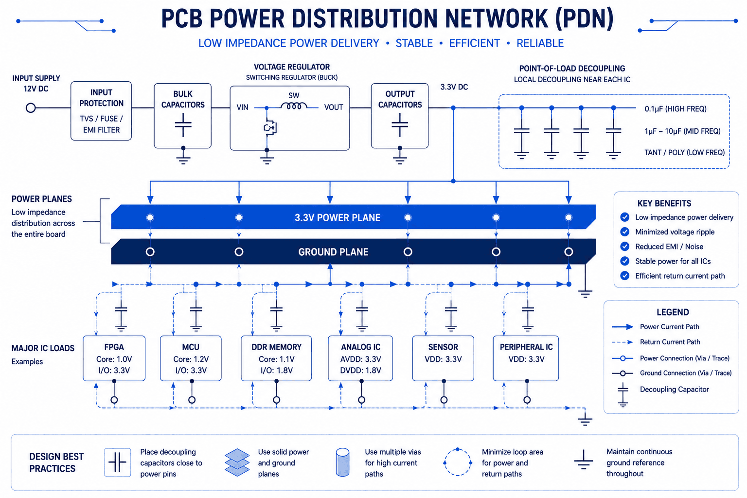
A reliable power distribution network ensures that every component receives a stable supply voltage under all operating conditions.
As modern electronics incorporate faster processors, high-current regulators, and mixed-voltage domains, PDN design has become increasingly important.
Poor PDN design can result in:
•
Excessive voltage drop
•
Power supply instability
•
Increased switching noise
•
Ground bounce
•
Electromagnetic interference
•
Reduced system reliability
The objective is to distribute power with low impedance while maintaining clean return paths and adequate decoupling.
Engineering Checklist – Power Distribution
Review the following before manufacturing:
Item | Verification |
|---|---|
Power Plane | Continuous where practical |
High-Current Paths | Short and adequately sized |
Voltage Drop | Within design limits |
Decoupling | Placed close to every major IC |
Grounding | Continuous reference planes maintained |
Plane Splits | Avoid crossing high-speed signals |
Current Density | Suitable for expected operating conditions |
Manufacturing Perspective
Designs with clearly organised power distribution are generally easier to fabricate, inspect, troubleshoot, and validate.
While the PCB fabricator manufactures copper exactly as designed, poor PDN architecture often becomes evident only during functional testing. Addressing these issues after fabrication usually requires a new PCB revision.
IPC Standard Reference
IPC-2152 – Determining Current-Carrying Capacity in Printed Board Design
Although many engineers continue to reference older conductor width charts, IPC-2152 provides more comprehensive guidance by considering copper thickness, board construction, thermal environment, and heat dissipation.
Using IPC-2152 during trace sizing leads to more realistic and reliable current-carrying calculations than relying on simplified historical tables alone.
Engineering Insight
Every milliohm of unnecessary resistance in the power distribution network contributes to voltage drop, heat generation, and reduced design margin. Good PDN design is an investment in long-term reliability.
6.10 Design for Thermal Management
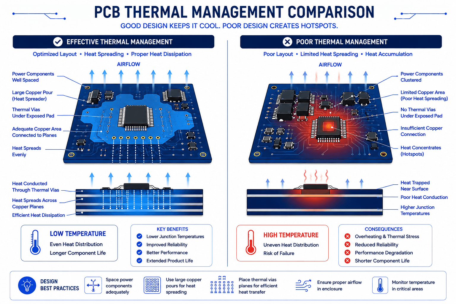
Electrical performance is only one aspect of a successful PCB design. Every watt of electrical power that is not converted into useful work becomes heat, and if that heat is not effectively managed, it can shorten component life, reduce system reliability, and cause intermittent failures that are extremely difficult to diagnose.
Thermal management should never be treated as a problem to solve after prototype testing. It should be considered during component placement, PCB stack-up planning, copper distribution, and airflow design.
Many products that function perfectly during laboratory testing fail prematurely in real-world environments because thermal behaviour was underestimated during design.
Sources of Heat in a PCB
Typical heat-generating components include:
•
Voltage regulators
•
MOSFETs
•
Power inductors
•
High-current connectors
•
Power resistors
•
High-performance processors
•
RF power amplifiers
•
LED drivers
The objective is not simply to dissipate heat, but to control its flow throughout the PCB.
Engineering Checklist – Thermal Design
Before manufacturing, verify:
✓ High-power components are identified.
✓ Heat sources are distributed rather than concentrated.
✓ Copper pours assist heat spreading.
✓ Thermal vias are provided beneath exposed thermal pads.
✓ Heat sinks have adequate mechanical clearance.
✓ Temperature-sensitive components are isolated from hot zones.
✓ Airflow direction has been considered.
✓ Thermal simulations or calculations have been reviewed where applicable.
Engineering Insight
Heat always follows the path of least thermal resistance. Good thermal design creates deliberate pathways that move heat away from sensitive components before temperatures become problematic.
Manufacturing Perspective
Adding a heat sink after prototype testing often solves only the symptom rather than the root cause. Good thermal performance begins with intelligent PCB layout.
Engineering Case Study
Thermal Vias Reduced Junction Temperature by 18°C
A motor controller PCB used a QFN package with an exposed thermal pad connected only by surface copper.
Initial testing revealed excessive device temperatures under continuous load.
The PCB was revised by:
•
Adding an array of thermal vias beneath the exposed pad.
•
Increasing the connected copper area.
•
Improving airflow around the power stage.
Subsequent testing showed an 18°C reduction in junction temperature without changing the component or adding an external heat sink.
Engineering Lesson
Small layout improvements often provide larger thermal benefits than expensive hardware modifications.
6.11 Use Vias Strategically
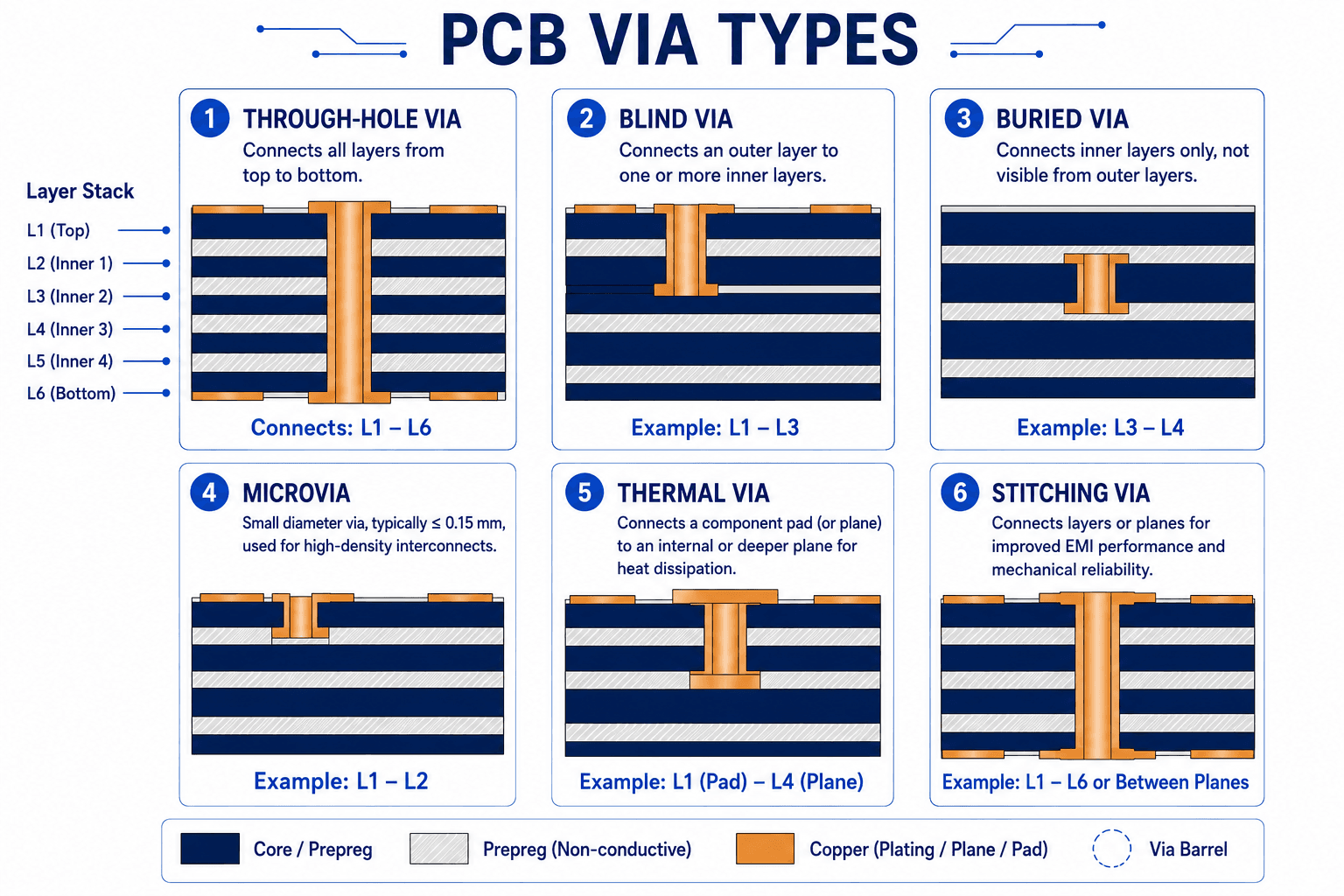
Vias are more than electrical connections between PCB layers. They influence routing flexibility, manufacturing complexity, thermal performance, signal integrity, and production cost.
A common mistake is to use vias simply wherever routing becomes difficult. Instead, vias should be placed deliberately and only where they add engineering value.
Different via technologies serve different purposes:
Via Type | Typical Application |
|---|---|
Through-hole Via | General signal and power routing |
Blind Via | High-density layouts where space is limited |
Buried Via | Internal interconnections in multilayer PCBs |
Microvia | HDI designs using laser drilling |
Thermal Via | Heat transfer beneath power devices |
Stitching Via | Ground continuity, EMI reduction, heat spreading |
Each technology carries different manufacturing implications and cost considerations.
Via Design Checklist
Review the following:
✓ Via sizes comply with manufacturer capabilities.
✓ Aspect ratios remain within recommended limits.
✓ Thermal vias are placed beneath power devices where appropriate.
✓ Ground stitching vias connect reference planes effectively.
✓ High-speed signal vias minimise unnecessary transitions.
✓ Via-in-pad is used only when manufacturing capability supports it.
Engineering Insight
Every via introduces electrical inductance and manufacturing complexity. Use vias intentionally rather than as a routing shortcut.
6.12 Design for Assembly (DFA)
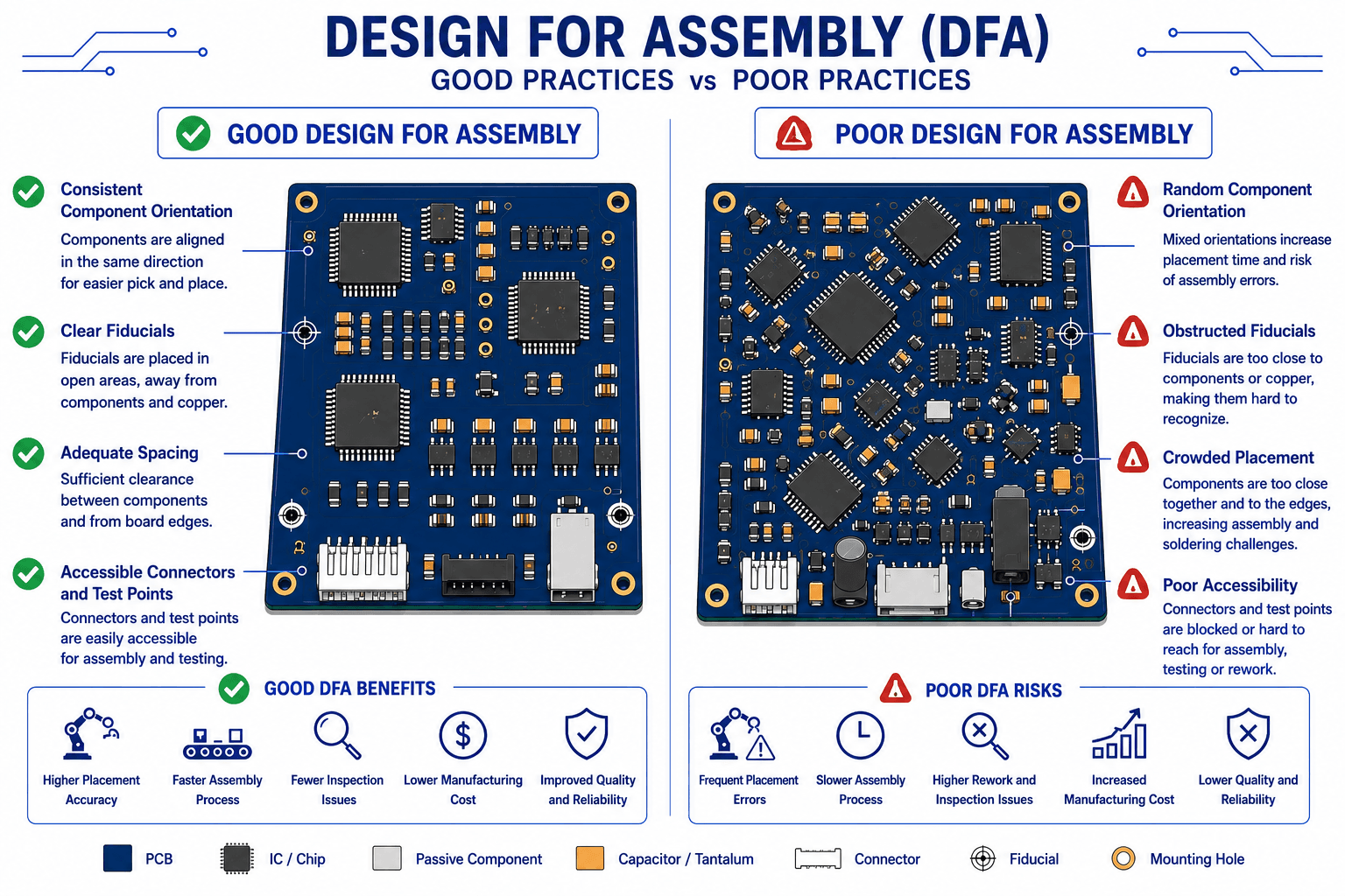
A PCB that can be fabricated successfully is only halfway to becoming a finished product. It must also be assembled efficiently, consistently, and economically.
Design for Assembly (DFA) focuses on ensuring that automated pick-and-place equipment, soldering processes, optical inspection systems, and manual rework can all be performed without unnecessary difficulty.
Ignoring DFA often results in:
•
Lower assembly yields.
•
Increased manual intervention.
•
Longer production times.
•
Higher manufacturing costs.
•
Greater risk of solder defects.
Best Practices for DFA
•
Maintain consistent orientation for polarized components.
•
Provide adequate spacing between components.
•
Avoid placing tall components where they obstruct inspection.
•
Keep fiducial marks unobstructed.
•
Maintain sufficient clearance around connectors and mechanical hardware.
•
Consider accessibility for future servicing and rework.
Manufacturing Perspective
Modern SMT production lines are highly automated. A layout that supports automation not only improves manufacturing efficiency but also enhances repeatability and product quality.
Engineering Case Study
Missing Fiducials Increased Setup Time
A medium-volume industrial controller was released without global fiducial marks.
Although the PCB was assembled successfully, each production batch required additional manual setup and alignment, increasing assembly time and reducing throughput.
Adding three simple fiducial marks in the next revision eliminated the issue entirely.
Engineering Lesson
Small features that appear insignificant during layout can have a substantial impact on production efficiency.
IPC Standard Reference
IPC-A-610 – Acceptability of Electronic Assemblies
IPC-A-610 is one of the most widely used standards for evaluating the quality and acceptability of assembled electronic products.
While it primarily guides inspection rather than PCB layout, understanding its acceptance criteria helps designers produce assemblies that are easier to manufacture and inspect successfully.
Engineering Insight
The most successful PCB designs are not simply easy to manufacture—they are easy to assemble, inspect, test, repair, and reproduce consistently at production scale.
6.13 Design for Testability (DFT)
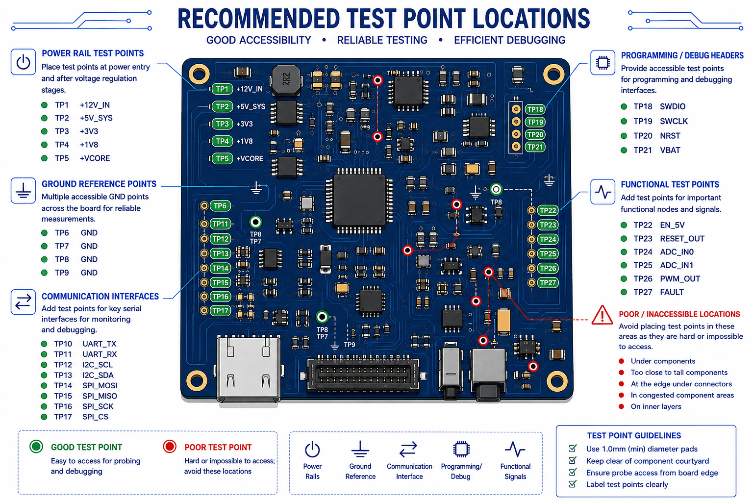
A PCB is not truly production-ready until it can be tested efficiently. Even the most carefully designed board can become expensive to manufacture if functional verification is slow, inconsistent, or overly dependent on manual intervention.
Design for Testability (DFT) ensures that production teams can verify electrical performance quickly and reliably during prototype validation, pilot builds, and volume manufacturing.
Testing should not be viewed as the final manufacturing step—it should be considered during the PCB layout phase.
Why DFT Matters
Every PCB leaving the production line should be capable of being verified against its design intent. Effective testability:
•
Detects manufacturing defects early
•
Reduces field failures
•
Improves production yield
•
Simplifies troubleshooting
•
Reduces warranty costs
•
Supports faster product introduction
Without adequate test access, even simple faults may require extensive manual investigation.
Engineering Checklist – Design for Testability
Before releasing the PCB, verify:
✓ Critical power rails have accessible test points.
✓ Programming interfaces remain accessible after assembly.
✓ Boundary scan (where applicable) has been considered.
✓ High-speed test connectors are correctly positioned.
✓ Test pads satisfy fixture requirements.
✓ Functional test strategy has been documented.
✓ Diagnostic LEDs and debug interfaces are included where appropriate.
✓ Test point labels are clearly documented.
Manufacturing Perspective
A design that cannot be tested efficiently often requires longer production cycles and increased operator involvement. Investing a small amount of PCB area in dedicated test access frequently reduces manufacturing cost over the product's lifetime.
Engineering Insight
A test point occupies only a few square millimetres on the PCB, but it can save hours of troubleshooting during production and field servicing.
Engineering Case Study
Limited Test Access Increased Production Time
A communications module reached pilot production without dedicated test points on several critical power rails. During functional failures, technicians were forced to probe fine-pitch component pins manually, increasing diagnosis time and introducing a risk of PCB damage.
In the next revision, clearly labelled test points were added for all major voltage rails and communication interfaces. Average troubleshooting time during production fell by more than 60%.
Engineering Lesson
Designing for testability improves both manufacturing efficiency and long-term serviceability.
6.14 Prepare Complete Manufacturing Documentation
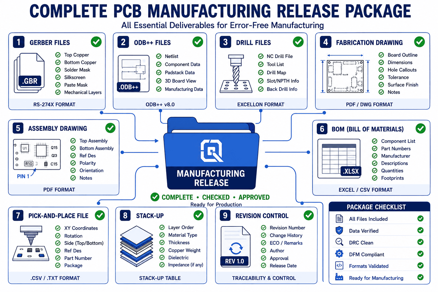
Even an excellent PCB layout can experience manufacturing delays if supporting documentation is incomplete or ambiguous.
Fabrication teams rely on manufacturing files to interpret the designer's intent. Missing notes, inconsistent file naming, or unclear fabrication instructions often result in engineering queries that delay production.
A complete release package should enable the manufacturer to begin fabrication without requiring clarification from the design team.
Manufacturing Documentation Checklist
Ensure the release package includes:
Document | Purpose |
|---|---|
Gerber or ODB++ Files | PCB fabrication data |
NC Drill Files | Hole drilling information |
Fabrication Drawing | Board dimensions, tolerances, materials, finishes |
Assembly Drawing | Component placement information |
Bill of Materials (BOM) | Component procurement and assembly |
Pick-and-Place File | Automated assembly coordinates |
Stack-up Information | Layer configuration and material details |
Fabrication Notes | Special manufacturing instructions |
Assembly Notes | Assembly process requirements |
Revision History | Traceability of engineering changes |
Engineering Insight
A PCB design is only as good as the documentation that accompanies it. Clear documentation reduces manufacturing questions, prevents interpretation errors, and accelerates production.
Manufacturing Perspective
Manufacturers frequently report that incomplete documentation—not fabrication capability—is one of the leading causes of production delays.
Investing additional time in documentation before release is significantly less expensive than resolving manufacturing queries after production has begun.
IPC Standard Reference
IPC-6012 – Qualification and Performance Specification for Rigid Printed Boards
IPC-6012 defines the qualification and performance requirements for rigid printed boards. It addresses aspects such as material quality, dimensional accuracy, plating integrity, conductor definition, and overall manufacturing acceptance.
Designers do not need to memorise every requirement, but understanding that fabrication quality is measured against recognised standards helps establish realistic expectations when selecting manufacturing partners.
6.15 Final Engineering Release Review
Before sending any design to manufacturing, conduct one final multidisciplinary review involving design, manufacturing, procurement, and quality stakeholders where possible.
This review should confirm not only that the design is electrically correct, but that it can also be fabricated, assembled, inspected, tested, and supplied consistently.
6.16 Final PCB Release Checklist
Design Verification
□ Electrical Rule Check (ERC) completed.
□ Design Rule Check (DRC) completed.
□ Stack-up verified.
□ Controlled impedance reviewed.
□ High-current traces validated.
□ Thermal analysis completed where applicable.
Mechanical Verification
□ Board outline confirmed.
□ Mounting holes verified.
□ Connector alignment checked.
□ Component height restrictions satisfied.
Manufacturing Readiness
□ Copper clearances verified.
□ Solder mask reviewed.
□ Silkscreen legibility confirmed.
□ Fiducials included.
□ Panelisation requirements reviewed.
□ Test points provided.
Documentation
□ Gerber or ODB++ package generated.
□ BOM validated.
□ Assembly drawing complete.
□ Fabrication drawing complete.
□ Revision number updated.
Supply Chain
□ Component availability confirmed.
□ Alternate components identified where appropriate.
□ Long lead-time items reviewed.
Quality Assurance
□ Manufacturing partner DFM review requested.
□ Internal engineering review completed.
□ Release approval documented.
7. Manufacturing Perspective
A structured release review transforms manufacturing from a transactional process into a collaborative engineering activity. Many production issues can be prevented simply by involving the manufacturing partner before fabrication begins.
8. Common PCB Design Mistakes Before Manufacturing
Even experienced engineers occasionally overlook details that affect manufacturability. The following issues are among the most frequently encountered during design reviews:
Mistake | Potential Impact |
|---|---|
Copper too close to board edge | Exposed copper after routing |
Missing fiducial marks | Slower SMT setup and inspection |
Inadequate decoupling placement | Power instability and EMI |
Split reference planes beneath high-speed signals | Signal integrity degradation |
Incomplete manufacturing documentation | Production delays |
Incorrect footprint dimensions | Assembly defects |
Poor thermal management | Component overheating |
Inaccessible test points | Difficult production testing |
Overly aggressive design rules | Reduced fabrication yield |
Ignoring manufacturer capabilities | Increased engineering queries and redesign |
9. Key Takeaways
•
Manufacturability begins during design, not after layout is complete.
•
A successful PCB balances electrical performance, mechanical integrity, thermal behaviour, manufacturability, and cost.
•
Early collaboration with manufacturing partners reduces redesigns and shortens time-to-market.
•
Industry standards such as IPC-2221, IPC-2152, IPC-6012, and IPC-A-610 provide valuable guidance, but should be complemented by manufacturer-specific capabilities.
•
A structured engineering review before release significantly improves first-pass manufacturing success.
10. Conclusion
Successful PCB manufacturing begins long before fabrication starts.
Every design decision—from defining product requirements and planning the layer stack-up to placing components, managing thermal performance, preparing manufacturing documentation, and validating testability—contributes to the overall success of the finished product.
The purpose of a PCB design checklist is not merely to avoid manufacturing defects. It is to establish a disciplined engineering process that delivers consistent quality, predictable production outcomes, and shorter development cycles.
By integrating Design for Manufacturability, Design for Assembly, and Design for Testability into every project, engineering teams can reduce redesigns, improve production yields, strengthen collaboration with manufacturing partners, and accelerate time-to-market.
Ultimately, a well-prepared PCB is easier to fabricate, simpler to assemble, more reliable in operation, and less expensive to produce over its entire lifecycle.
Whether you are developing a proof of concept, a low-volume industrial controller, or a high-volume consumer product, a structured engineering review before release remains one of the most valuable investments you can make.
Frequently Asked Questions
Ready to manufacture your electronics project?
Upload your Gerber files & BOM for automated DFM review, engineering feedback, and guaranteed delivery timelines.