
Why Partner
With Us.
Predictability. Communication. Execution.
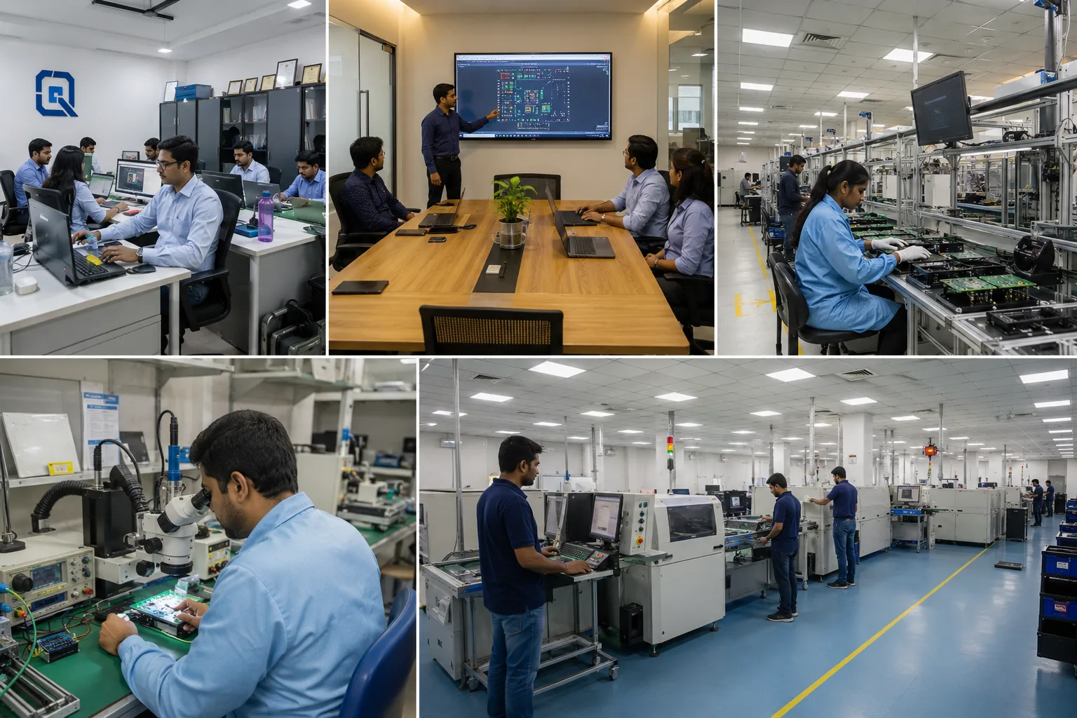
Projects are handled as coordinated engineering workflows rather than transactional manufacturing requests. We ensure design, sourcing, and manufacturing remain perfectly aligned.
A Structured, Engineer-Led Workflow
How It Works
What This Means
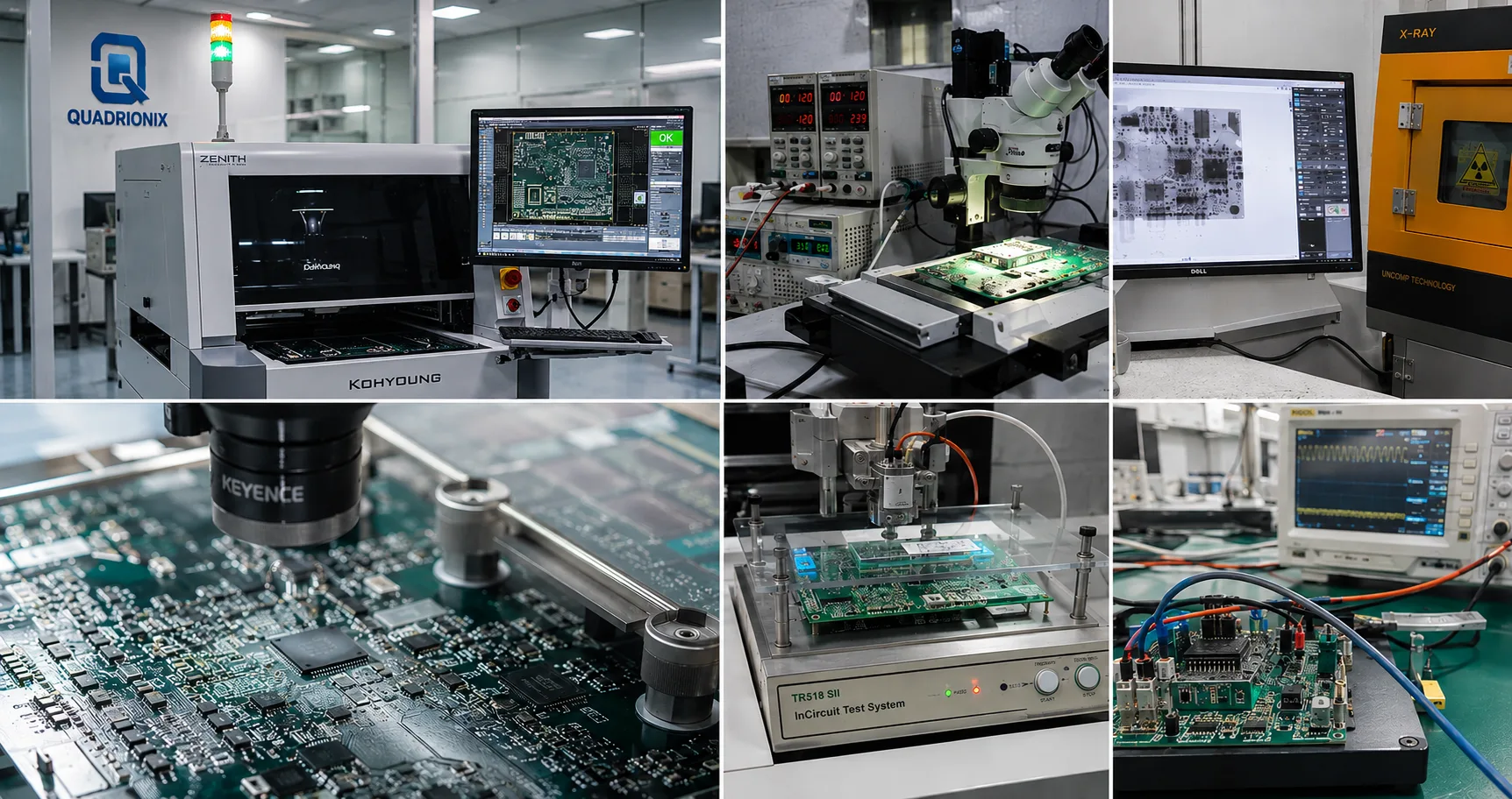
Quality Built Through Process
Process Approach
Inspection & Validation (Where Applicable)
The Advantage.
Strategic capabilities that define our execution model, ensuring absolute predictability and quality at every single stage of production.

Engineering-Aligned Execution
Pre-production engineering review and DFM validation to eliminate rework cycles, production issues, and manufacturing delays before release.

Design → Manufacturing → Validation Alignment
Complete synchronization across schematic layout, board fabrication, and automated testing to maximize first-pass yield.

Single-Point Coordination
A single consolidated engineering workflow managing fabrication, assembly, and component sourcing without vendor communication gaps.

IP Protection & Confidentiality
NDA-ready workflows, restricted file access, and secure documentation protocols to protect your proprietary hardware IP.

Flexible Execution Model
Adaptive manufacturing lanes tailored for specialized technology thresholds, custom builds, and volume scaling.

Transparent & Structured Process
Defined requirements, structured milestone tracking, and transparent communication across all production stages.

Global Delivery & Communication
Export-ready packaging, international customs support, and structured coordination aligned with global time zones.
Lifecycle & ObsolescenceContinuous Audit
Alternate Sourcing NetworkPre-Verified
Lead-Time Volatility ControlActive Buffer
Supply Chain & BOM Risk Control
Proactive BOM validation, component lifecycle analysis, and alternate sourcing strategies to mitigate supply chain volatility.
Prototype Validation1 – 50 pcs
Pilot Production50 – 1k pcs
Volume Scaling1k – 10k+ pcs
Focus on Controlled Builds
Disciplined process control optimized for high-mix prototype validation, pilot production, and precision volume manufacturing.
What You Can Expect
Engineering-led evaluation before execution, predictable manufacturing outcomes, reduced iteration cycles, and absolute alignment between design intent and physical output.
Engineering-Led
Manual DFM validation before execution.
Controlled Yield
Zero unverified component changes.
Global Traceability
Export packaging and documentation.

Why भारत / India for Electronics Manufacturing
India offers a strong combination of engineering capability and manufacturing depth, offering a strong engineering talent base, expanding electronics ecosystem, supply chain resilience, and alignment with global standards.
Strong Engineering Talent Base
Deep pool of hardware, embedded, and DFM engineers capable of handling complex design-to-manufacturing transitions.
Expanding Electronics Ecosystem
Rapidly growing infrastructure for high-precision PCB fabrication, advanced SMT assembly, and component sourcing.
Supply Chain Resilience
Strategic diversification and global supply chain integration providing reliable manufacturing alternatives.
Alignment with Global Standards
Full alignment with international quality specifications (IPC, ISO, CE) and export-ready delivery workflows.
OUR ENGINEERING MASTERPIECES.
See what we can build.
Engineering Engagements: Quadrionix Approach
Many electronics projects are protected by customer non-disclosure obligations. The representative examples given here illustrates typical projects and engineering approach typically taken by Quadrionix.
Industrial Automation
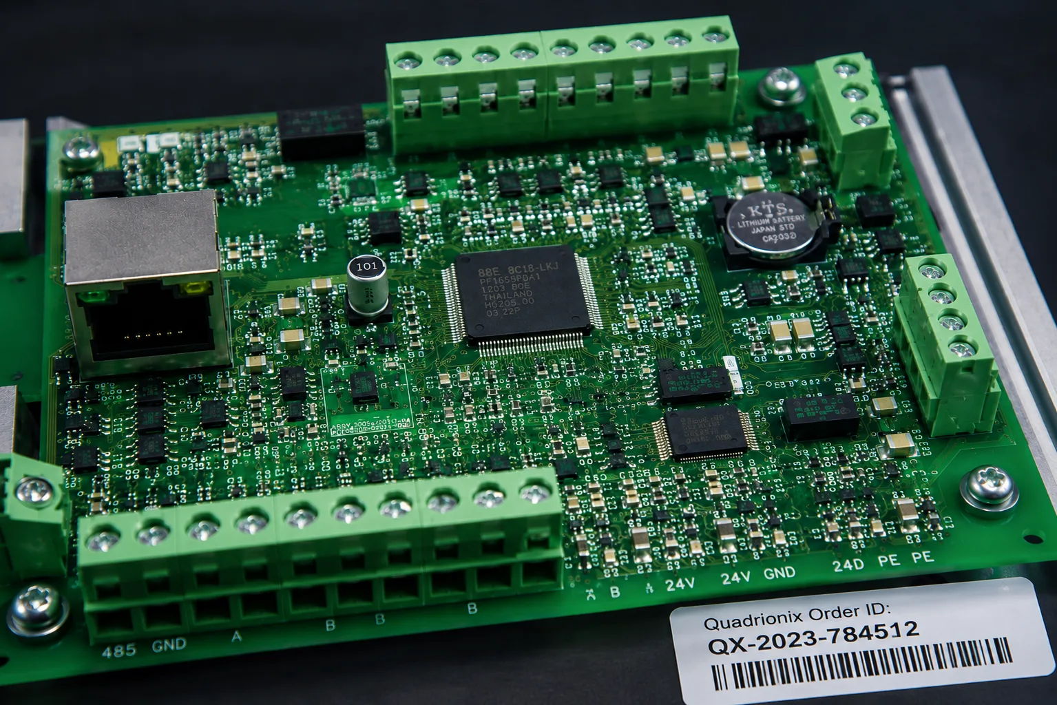
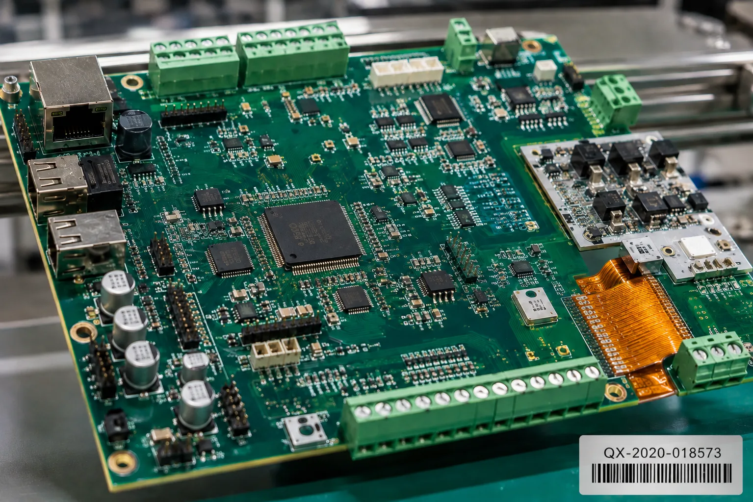
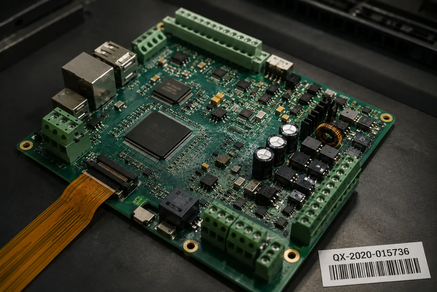
A compact industrial controller PCB required controlled-impedance routing for high-speed communication interfaces, galvanic isolation between power and control domains, multiple fine-pitch ICs, and efficient thermal dissipation within a constrained enclosure. The design also needed to support rapid prototype iterations without compromising manufacturability or assembly yield.
The engineering workflow included stack-up optimisation, impedance verification, DFM and DFA review, fabrication capability assessment, component lifecycle analysis, stencil aperture optimisation, SMT process planning, AOI inspection strategy, and prototype production readiness evaluation before manufacturing release.
Medical Electronics
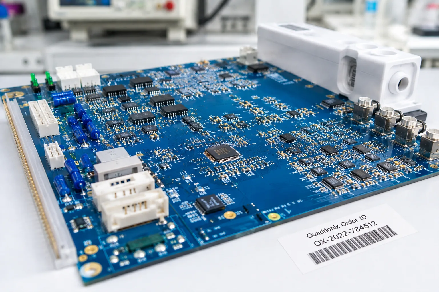
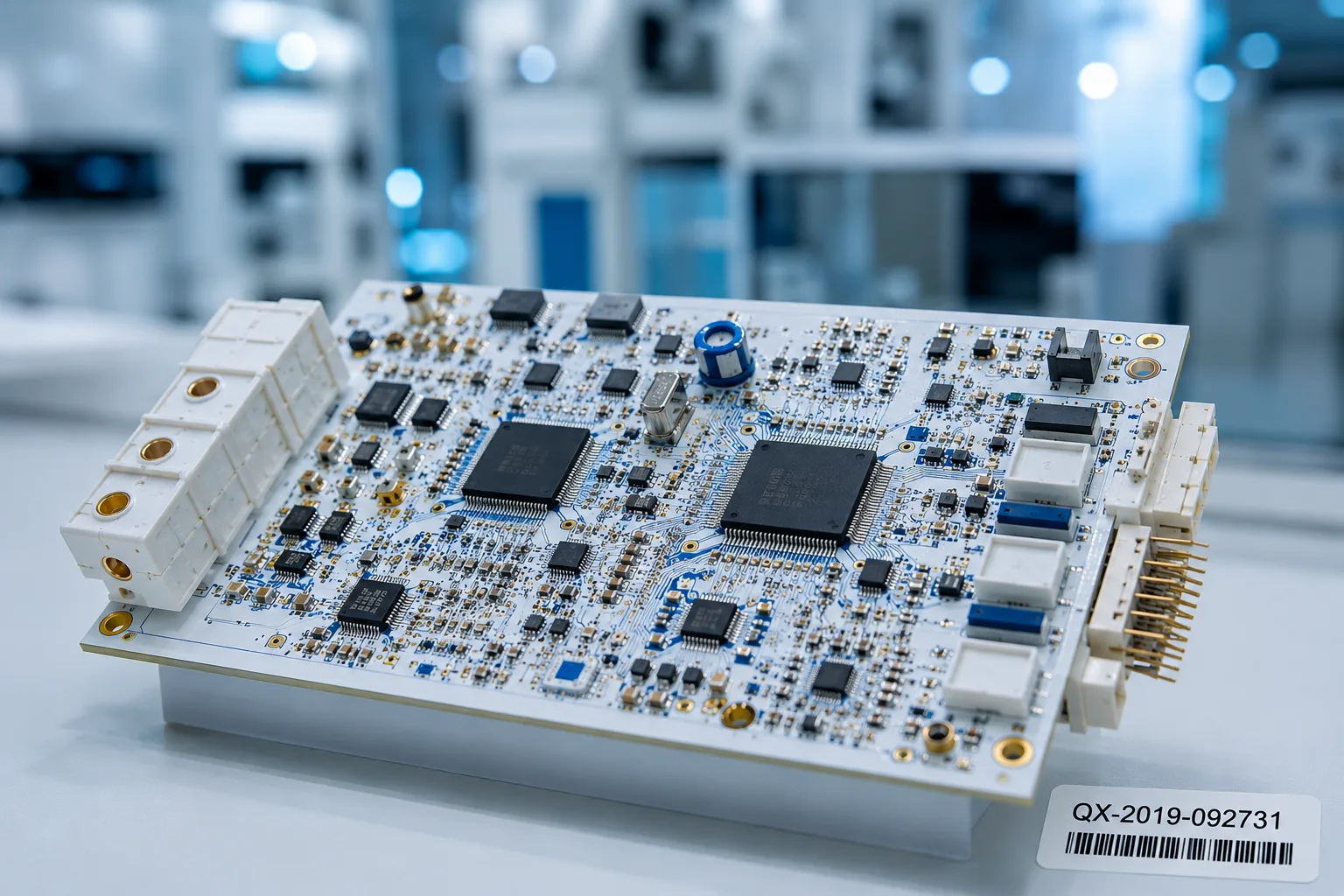
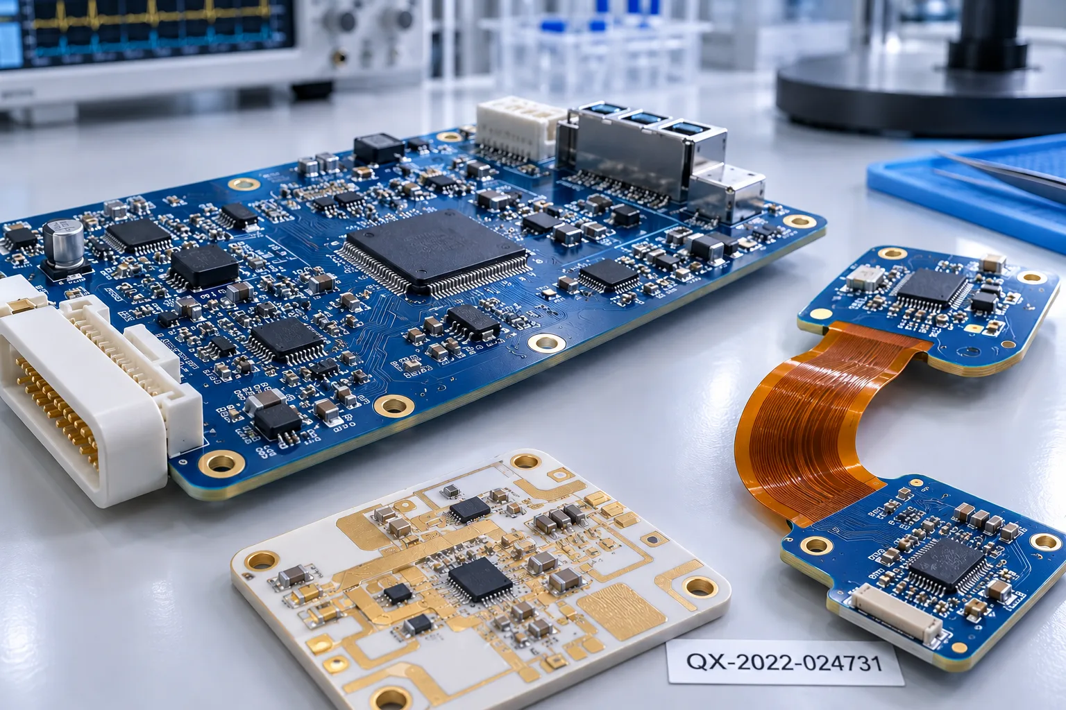
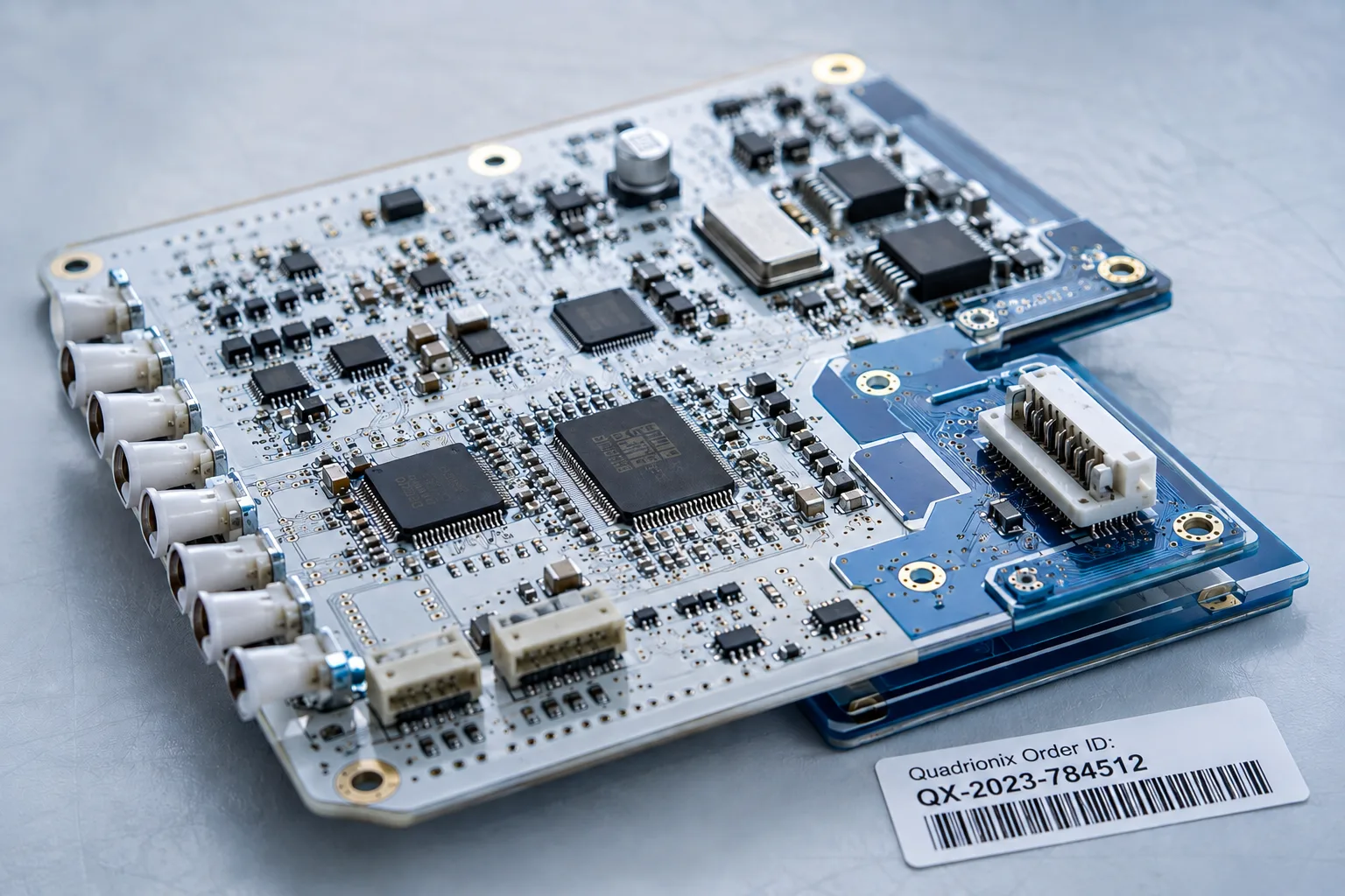
A compact medical electronics module required precision analog signal acquisition, low-noise PCB layout, stable power distribution, and reliable assembly of fine-pitch mixed-signal components. Manufacturing documentation and inspection planning were critical to support repeatable prototype validation and future design transfer activities.
Engineering activities included PCB layout manufacturability review, analog ground partition verification, component placement optimisation, solderability assessment, AOI inspection planning, X-ray inspection evaluation for hidden solder joints where applicable, controlled documentation management, and structured prototype build coordination.
IoT & Smart Devices
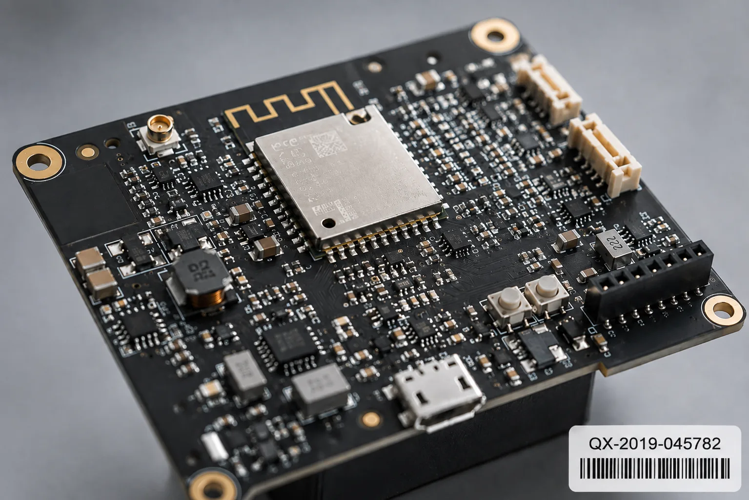
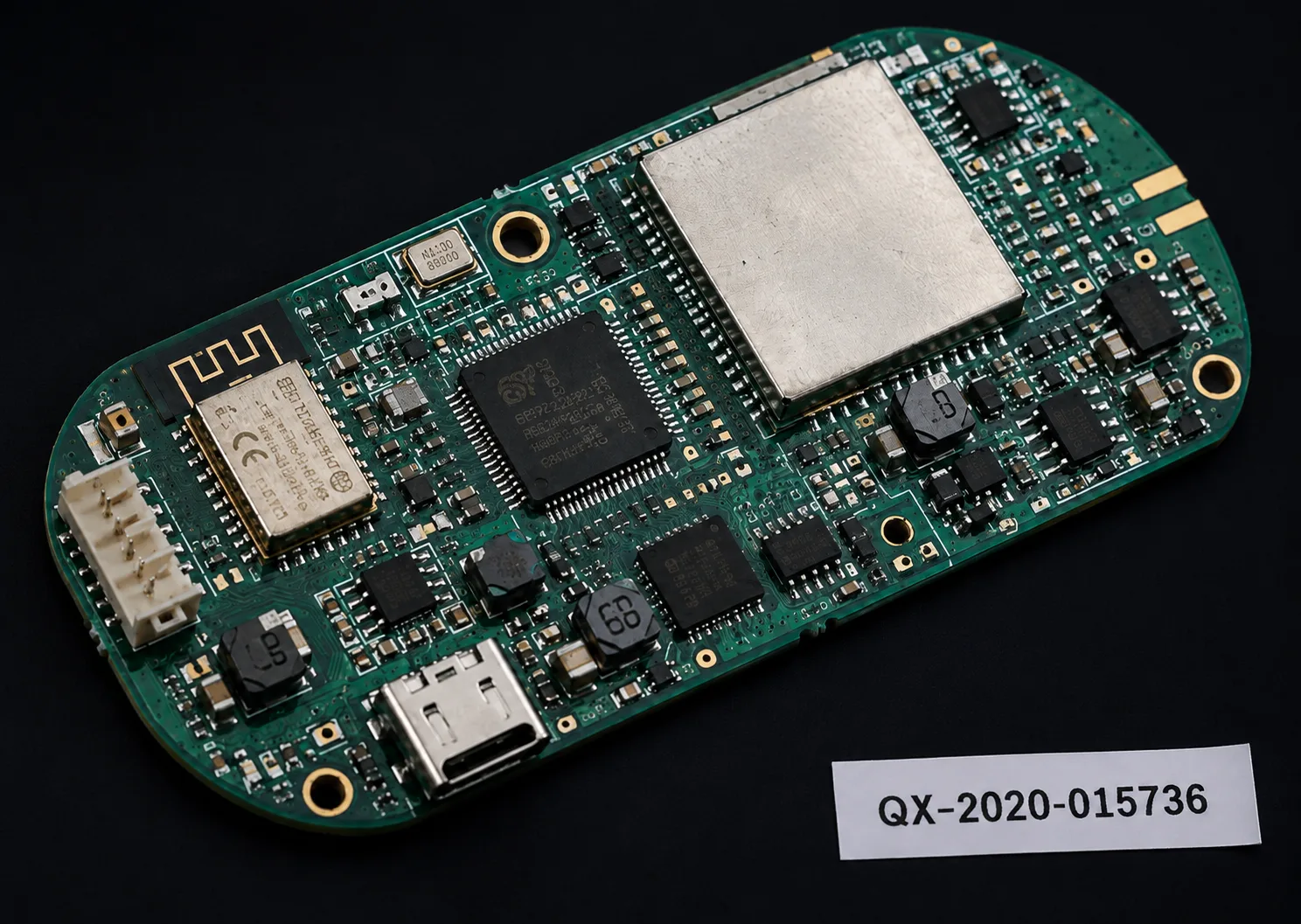
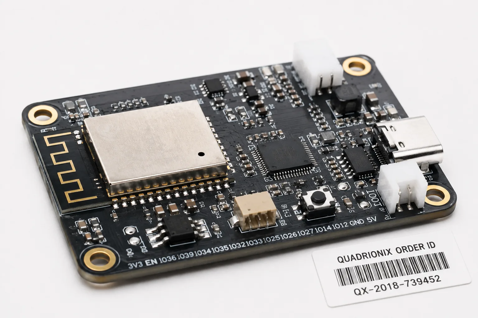
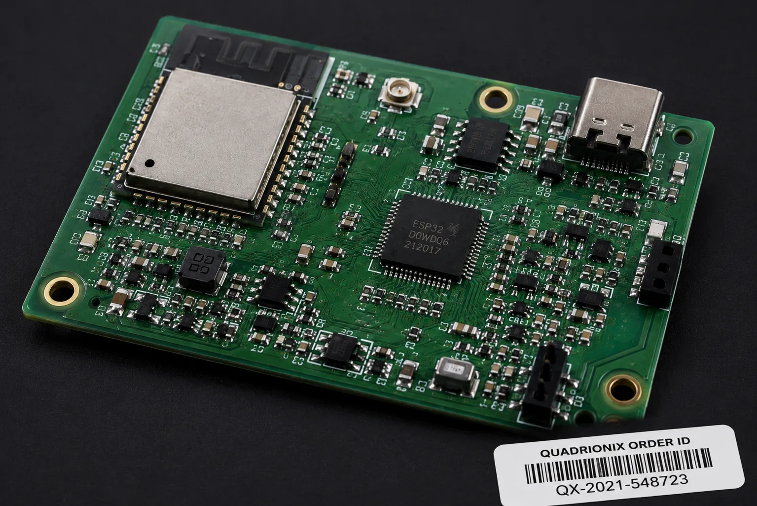
A compact IoT communication module required high-density routing around RF circuitry, controlled antenna clearance, low-power architecture, compact board dimensions, and rapid component sourcing despite lifecycle uncertainty for several wireless communication devices.
Engineering review focused on RF layout manufacturability, PCB stack-up optimisation, BOM risk analysis, alternate component identification, assembly process validation, stencil optimisation for miniature passive components, inspection workflow planning, and coordinated prototype manufacturing.
Automotive Electronics
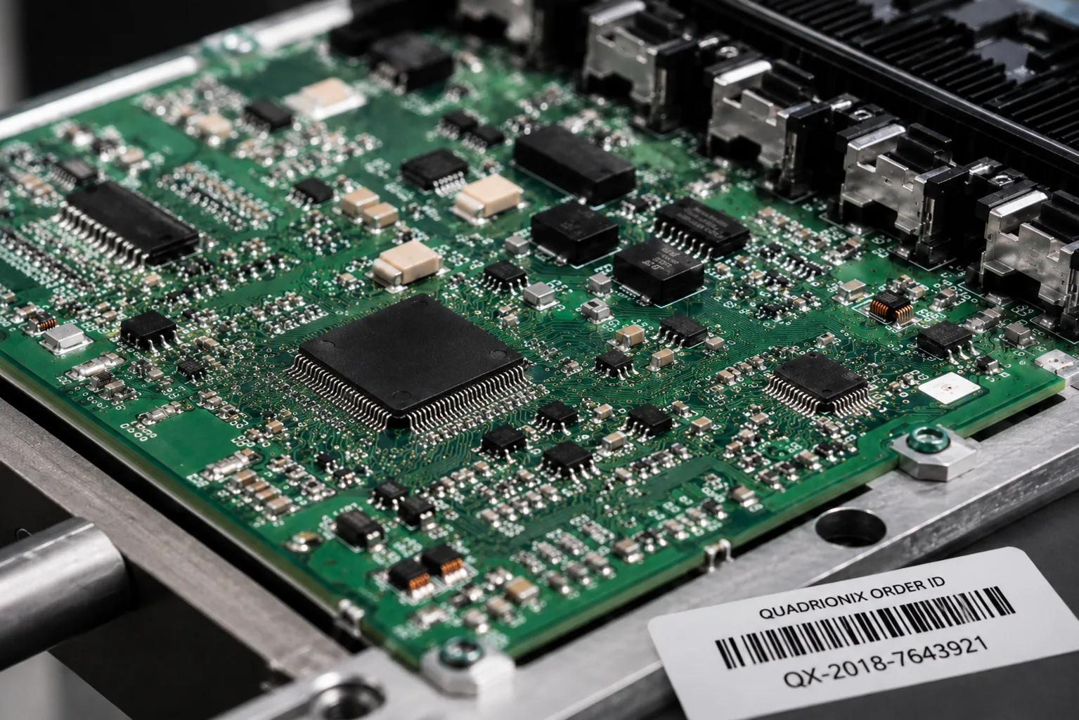
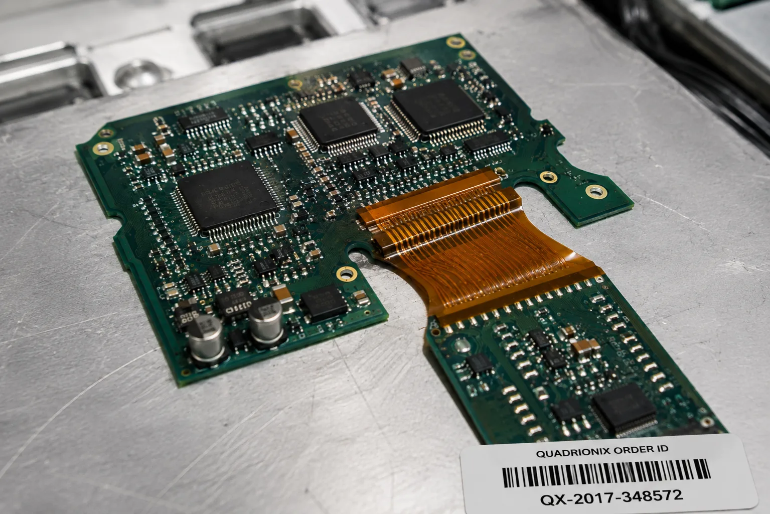
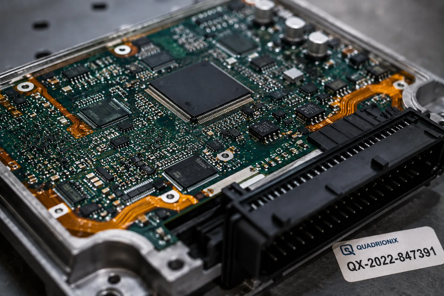
An automotive electronic control module required reliable multilayer PCB construction capable of supporting high component density, vibration-resistant assembly, controlled power distribution, and stable operation across extended temperature variations while maintaining efficient prototype manufacturing schedules.
Engineering activities included manufacturability assessment, PCB stack-up verification, thermal management review, solder joint reliability evaluation, assembly process planning, inspection strategy definition, prototype build coordination, and production readiness validation.
Aerospace & Avionics
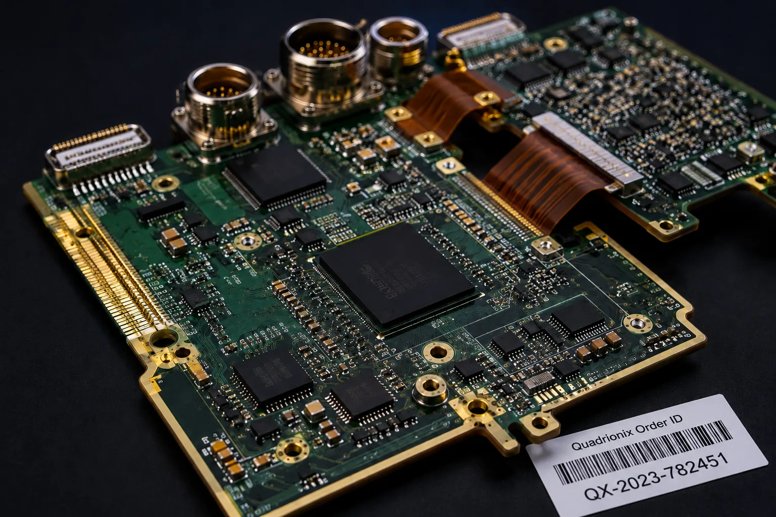
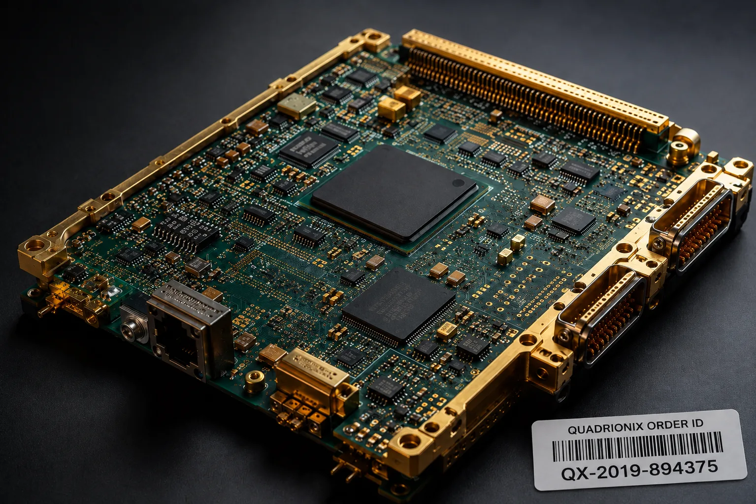
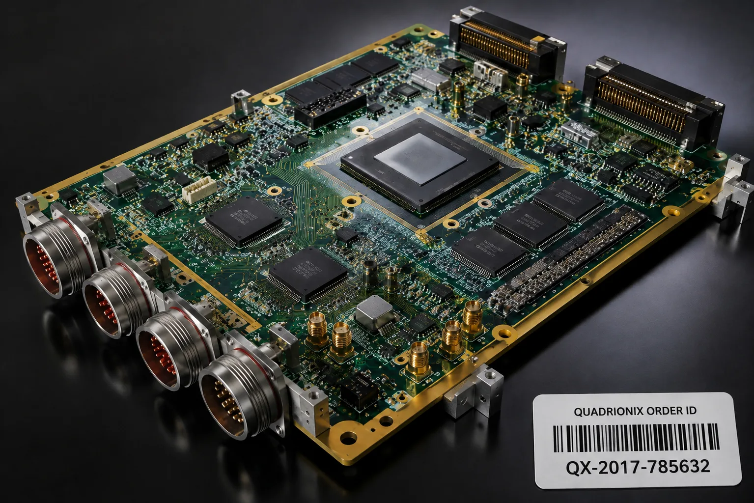
A high-density avionics control PCB required multilayer signal routing, strict impedance control, complex BGA package integration, high connector density, and manufacturing processes capable of supporting demanding reliability expectations throughout prototype development.
Engineering review included controlled stack-up validation, signal integrity assessment, fabrication process planning, BGA assembly evaluation, inspection methodology definition, documentation control, DFM review, and structured manufacturing readiness assessment before prototype release.
Defence Electronics
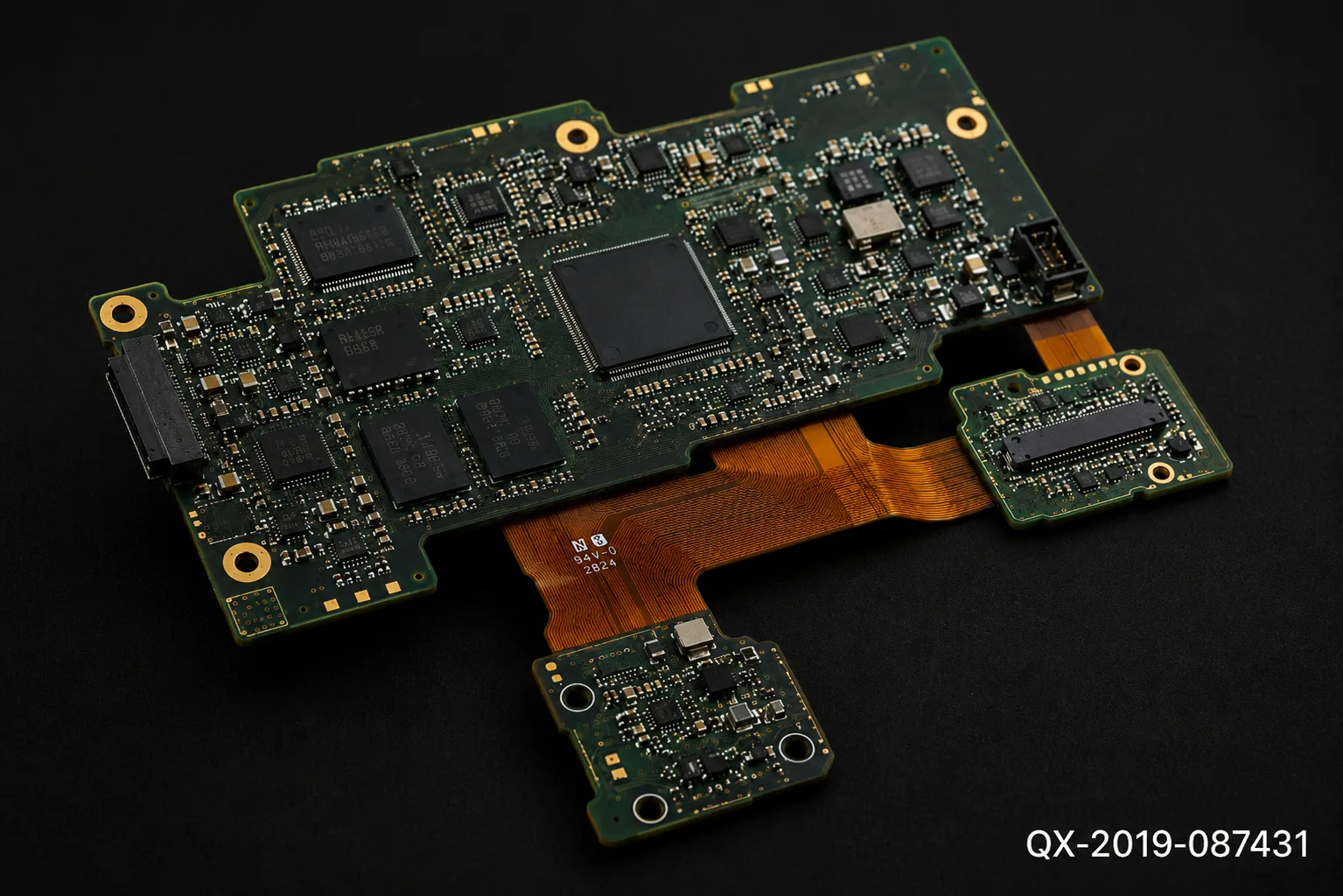
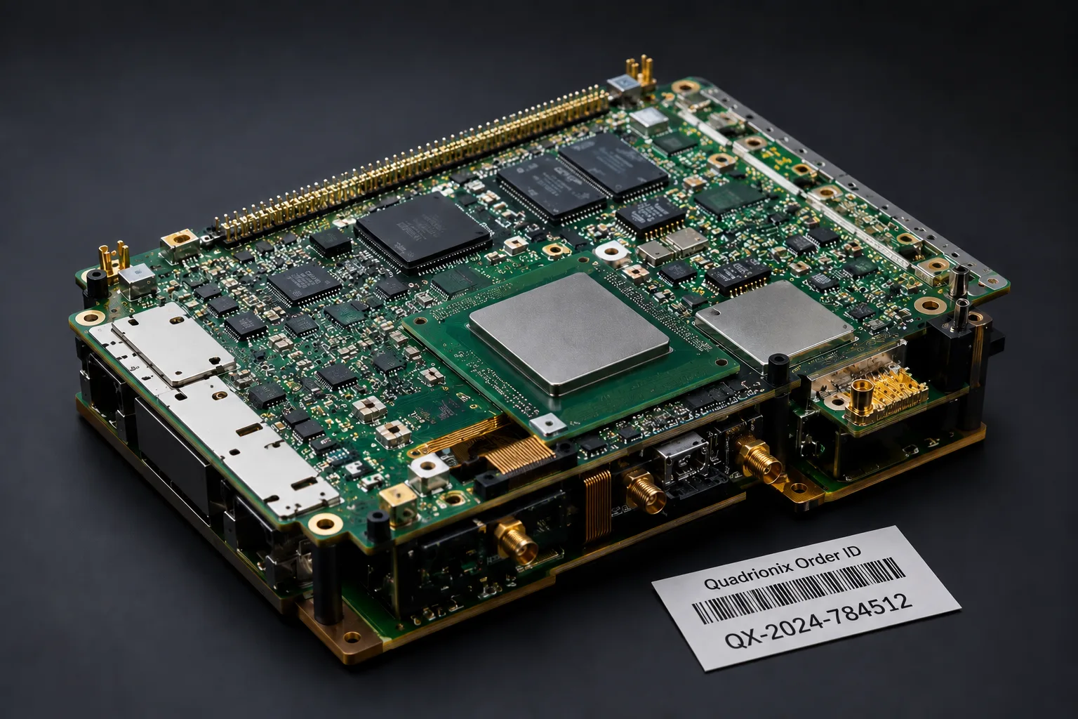
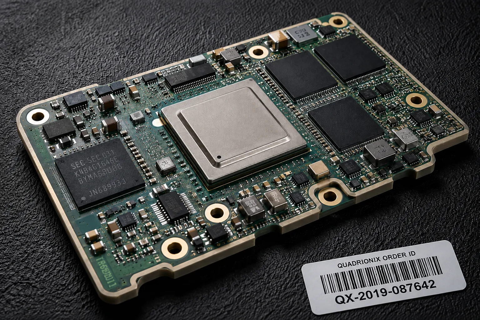
A rugged embedded electronic module required dense multilayer PCB architecture, high-speed digital interfaces, robust power integrity, reliable SMT assembly of fine-pitch devices, and disciplined manufacturing processes capable of supporting harsh operating environments while maintaining configuration control.
Engineering activities included PCB manufacturability assessment, stack-up optimisation, signal and power integrity review, fabrication planning, assembly process validation, AOI inspection planning, documentation control, prototype coordination, and structured production readiness evaluation.