Controlled Impedance Basics for PCB Designers
A practical guide to impedance-controlled PCB design, stack-up selection, trace geometry, tolerances and fabrication considerations

Controlled impedance PCB design showing high-speed traces and multilayer stack-up
As PCB data rates increase, the electrical behavior of a PCB trace becomes increasingly important.
At lower frequencies, designers can often think of a PCB trace primarily as a connection between two components.
At sufficiently high signal speeds, that assumption breaks down.
The trace itself becomes part of the electrical system.
Its:
can all influence signal behavior.
This is where controlled impedance PCB design becomes important.
Controlled impedance is the practice of designing and manufacturing PCB transmission lines so that their characteristic impedance stays within a defined target and tolerance.
Typical examples include:
50 Ω single-ended
and
90 Ω or 100 Ω differential
depending on the interface and system requirements.
But impedance control is not simply a matter of entering a trace width into a calculator.
It is a collaboration between:
PCB design → stack-up → materials → fabrication → verification
This article explains the fundamentals.
1. What Is PCB Impedance?
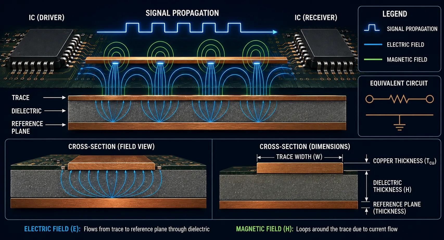
At high signal speeds, a PCB trace behaves as a transmission line rather than simply an electrical connection.
In simple terms, impedance describes how a transmission line responds to a changing electrical signal.
For PCB transmission lines, characteristic impedance is influenced by the geometry of the trace and the surrounding dielectric structure.
Unlike ordinary DC resistance, impedance is strongly associated with signals that vary with time and frequency.
For high-speed signals, the relationship between:
Signal + Trace + Dielectric + Reference Plane
becomes important.
A PCB trace therefore needs to be considered as part of the transmission-line system.
2. What Does "Controlled Impedance" Mean?
Controlled impedance means designing the PCB transmission line so its characteristic impedance is maintained within a specified target and tolerance.
For example, a design may specify:
50 Ω ±10%
This means the intended impedance range is approximately:
45 Ω to 55 Ω
for the specified transmission line.
The actual requirement depends on the interface and system design.
The important point is that the PCB manufacturer must understand:
What impedance is required, where it applies and what tolerance is acceptable.
3. Why Does Controlled Impedance Matter?
Signal integrity can become increasingly sensitive as signal transition times become faster.
Poorly controlled transmission-line characteristics can contribute to phenomena such as:
The consequence can range from reduced signal margin to complete system failure.
This is why controlled impedance is particularly important in high-speed interfaces.
4. When Does a PCB Need Controlled Impedance?
Not every PCB trace needs impedance control.
The requirement depends on factors such as:
Common applications where impedance-controlled routing may be important include:
The correct question is therefore not:
"Is this PCB high frequency?"
but rather:
"Does this interconnect behave as a transmission line for the signal being carried?"
5. Single-Ended vs Differential Impedance
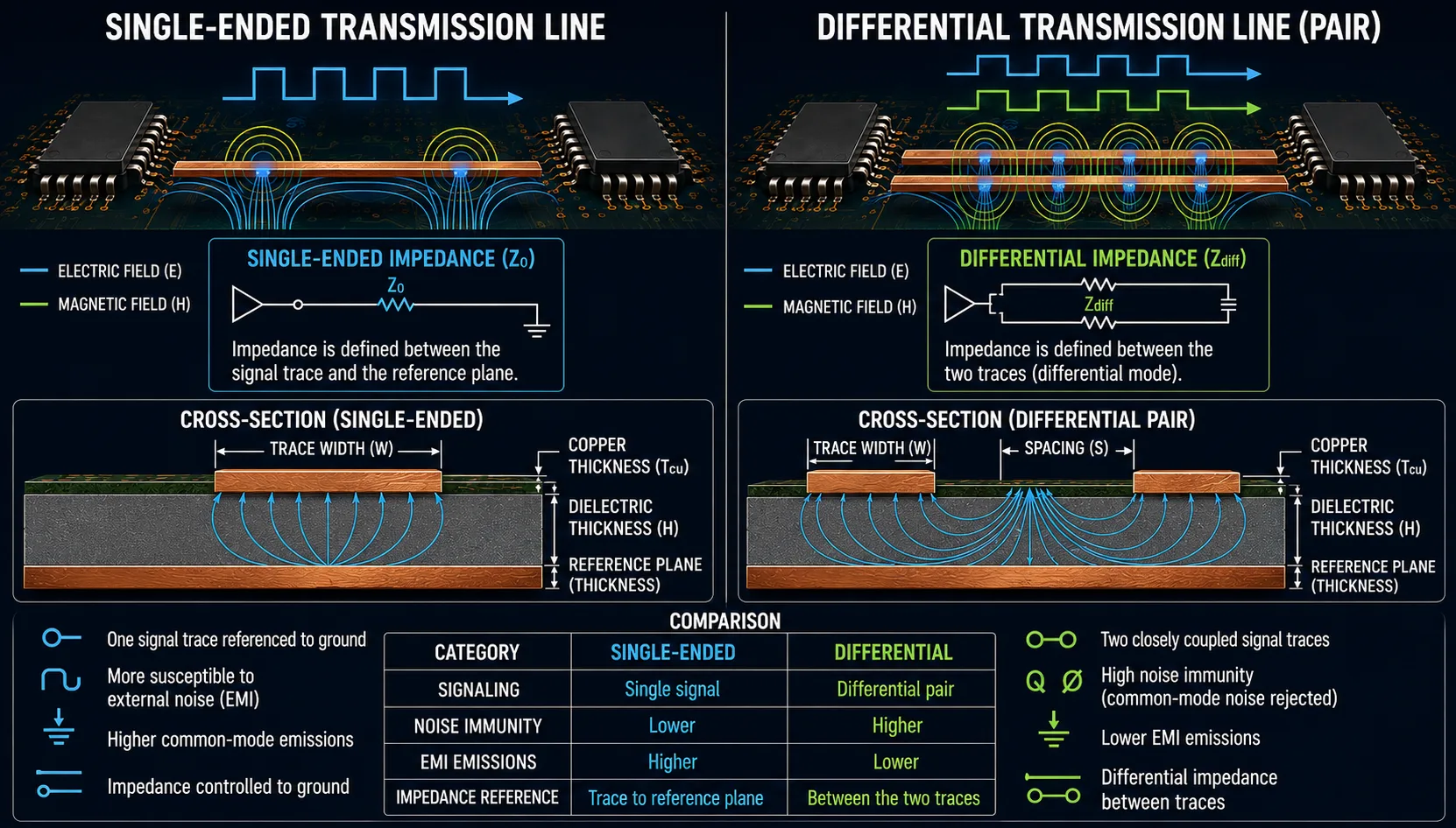
Single-ended and differential transmission lines depend on different geometric relationships and should be specified separately.
One of the first distinctions PCB designers need to understand is between single-ended and differential impedance.
Single-Ended Impedance
A single-ended transmission line is referenced to a nearby reference plane.
A commonly encountered target is:
50 Ω
The exact value depends on the interface and system architecture.
Differential Impedance
A differential pair consists of two traces carrying complementary signals.
The impedance is defined between the two conductors as a pair.
Common design targets include:
90 Ω differential
or
100 Ω differential
depending on the interface.
The target should come from the interface or system specification—not from a generic rule.
6. What Determines PCB Trace Impedance?
Several physical variables influence controlled impedance.
The most important include:
Trace width
Wider or narrower traces influence impedance.
Copper thickness
The conductor thickness affects the electromagnetic geometry.
Dielectric thickness
The distance between the signal trace and reference plane is important.
Dielectric constant
The electrical properties of the PCB material influence impedance.
Trace-to-trace spacing
For differential pairs, coupling between the traces depends strongly on spacing.
Reference-plane configuration
The signal's relationship to its reference plane affects the transmission-line structure.
Trace geometry
Microstrip, stripline and other structures have different impedance characteristics.
7. Trace Width Matters
Trace width is one of the most visible variables in impedance control.
Changing trace width changes the electromagnetic field distribution and therefore the characteristic impedance.
This means a designer cannot arbitrarily change a controlled-impedance trace from:
4 mil → 6 mil
without considering the impedance consequences.
The final width should be determined from the intended stack-up and impedance requirement.
8. Dielectric Thickness Matters
The distance between a signal trace and its reference plane is another major variable.
For example, a thinner dielectric layer between the signal and reference plane produces a different impedance than a thicker dielectric layer.
This is one reason PCB stack-up selection should occur early in the design process.
9. PCB Material Matters
The dielectric properties of the PCB material influence transmission-line behavior.
Important parameters can include:
For demanding high-speed designs, using a material based only on its nominal "FR-4" designation may not provide sufficient information.
The designer and manufacturer may need to work with more specific material characteristics.
10. Why Stack-Up Is Critical
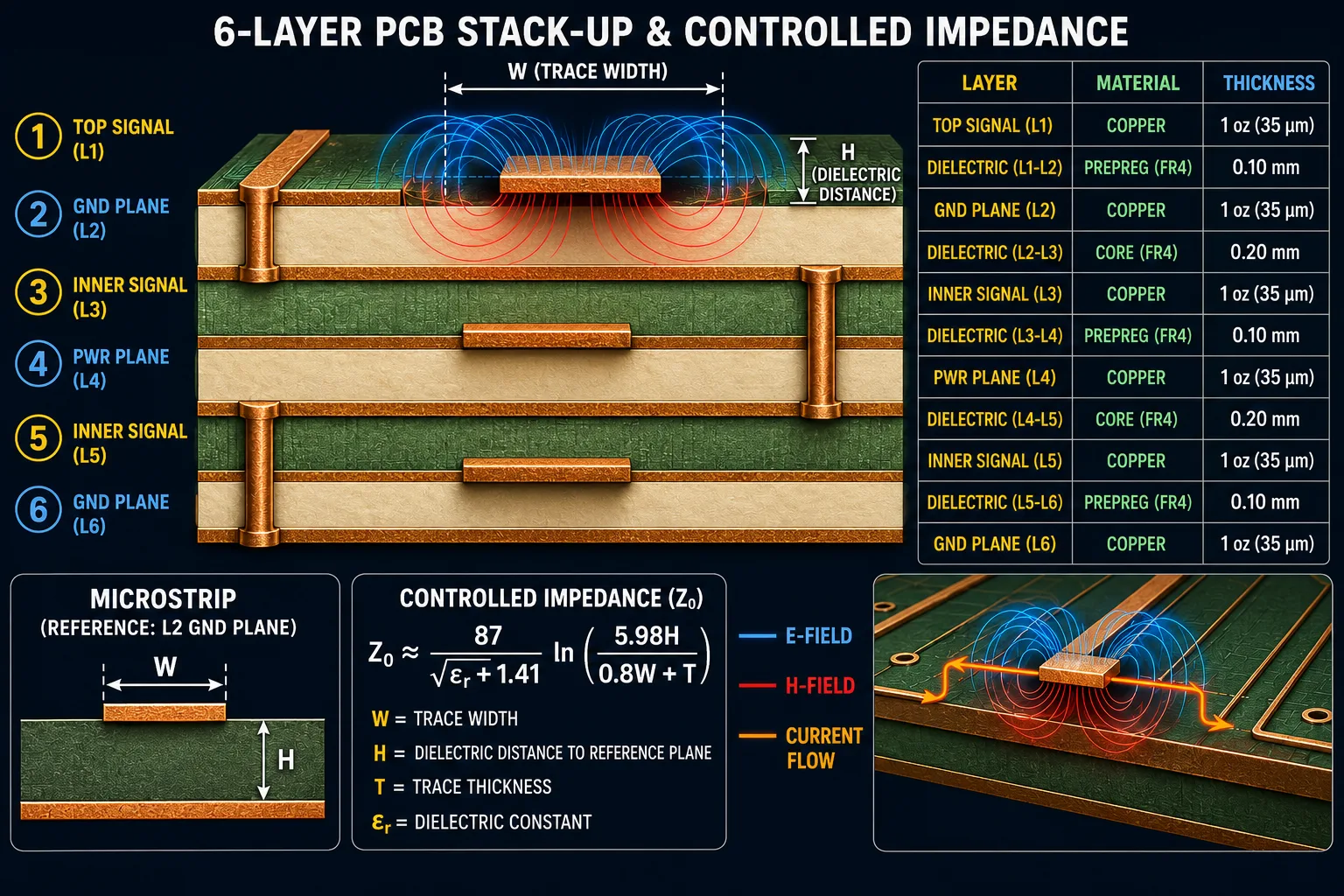
Controlled impedance is a property of the complete transmission-line geometry, not simply the trace width.
Controlled impedance is fundamentally connected to the PCB stack-up.
For a multilayer PCB, the stack-up defines:
Changing the stack-up can change the impedance of an existing trace.
Therefore:
Do not finalize controlled-impedance trace widths before the relevant stack-up has been established.
11. Microstrip vs Stripline
Two common PCB transmission-line structures are:
Microstrip
The signal trace is located on an outer layer with a reference plane beneath it.
Stripline
The signal trace is located between reference planes within the PCB structure.
Their electromagnetic environments are different.
Consequently, the same trace width will not necessarily produce the same impedance in both structures.
12. Differential Pair Geometry Matters
For differential pairs, impedance is affected by the relationship between the two traces.
Important parameters include:
The spacing between the traces affects their coupling.
Changing pair spacing can therefore change differential impedance.
13. Do Differential Pairs Need to Be Perfectly Equal?
For many high-speed differential interfaces, maintaining good pair symmetry is important.
Designers should pay attention to:
However, length matching alone does not guarantee signal integrity.
The complete routing environment matters.
14. Reference Planes Are Critical
A controlled-impedance trace needs an appropriate return-current path.
A continuous reference plane can provide a predictable electromagnetic environment.
Routing across:
can create problems even if the trace itself was calculated correctly.
Therefore:
Impedance control is not only about the signal trace. It is about the complete signal-and-return structure.
15. Vias Can Create Impedance Discontinuities
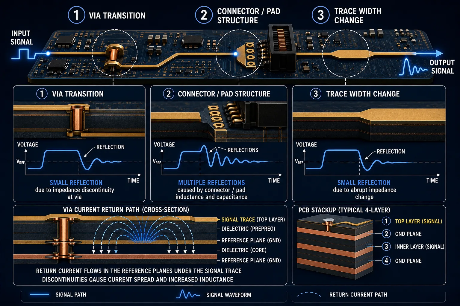
Connectors, vias, pads and abrupt geometry changes can introduce impedance discontinuities in high-speed signal paths.
A signal that transitions between PCB layers through a via does not encounter exactly the same geometry as the horizontal trace.
The transition can introduce:
For demanding high-speed designs, via structures may need specific attention.
Potential techniques include:
The appropriate solution depends on the interface and design requirements.
16. Connectors Also Matter
The PCB trace may have carefully controlled impedance, but the signal path does not end at the trace.
Connectors, cables and packages can introduce their own impedance characteristics.
For high-speed systems, designers should therefore consider the entire interconnect:
IC → Package → Via → PCB Trace → Connector → Cable → Receiver
rather than evaluating the PCB trace in isolation.
17. Don't Use a Generic "50 Ω Trace Width"
One of the most common mistakes is asking:
"What trace width gives me 50 Ω?"
There is no universal answer.
A 50 Ω trace might require different widths depending on:
A trace width that produces 50 Ω on one PCB may produce a substantially different impedance on another.
18. Impedance Calculators Are Useful—but Not the Whole Story
PCB design software and impedance calculators can estimate trace geometry.
They are valuable during design.
But the calculated value is based on assumptions.
The fabricated PCB can differ because of:
Therefore, controlled impedance is ultimately a design + fabrication problem.
19. Work With the Fabricator Early
For a controlled-impedance PCB, the PCB manufacturer should ideally be involved before the design is finalized.
The designer can provide:
The fabricator can then review the proposed stack-up and manufacturing capability.
This can prevent a situation where the designer creates a theoretically correct design that is difficult to manufacture consistently.
20. The Manufacturer May Need to Adjust the Stack-Up
In some cases, the buyer specifies the impedance requirement but allows the manufacturer to optimize the construction.
For example:
50 Ω ±10% on specified signal layers
with the fabricator proposing an appropriate stack-up.
This can provide greater manufacturing flexibility.
However, if the stack-up is already fixed by the design, the manufacturer should not change it without engineering approval.
21. Define Impedance Tolerance
"50 Ω controlled impedance" is incomplete unless the acceptable tolerance is understood.
Examples might include:
The appropriate tolerance depends on the interface and system requirements.
Tighter tolerance can place greater demands on:
Therefore, specify the tolerance based on actual engineering requirements.
22. Impedance Testing
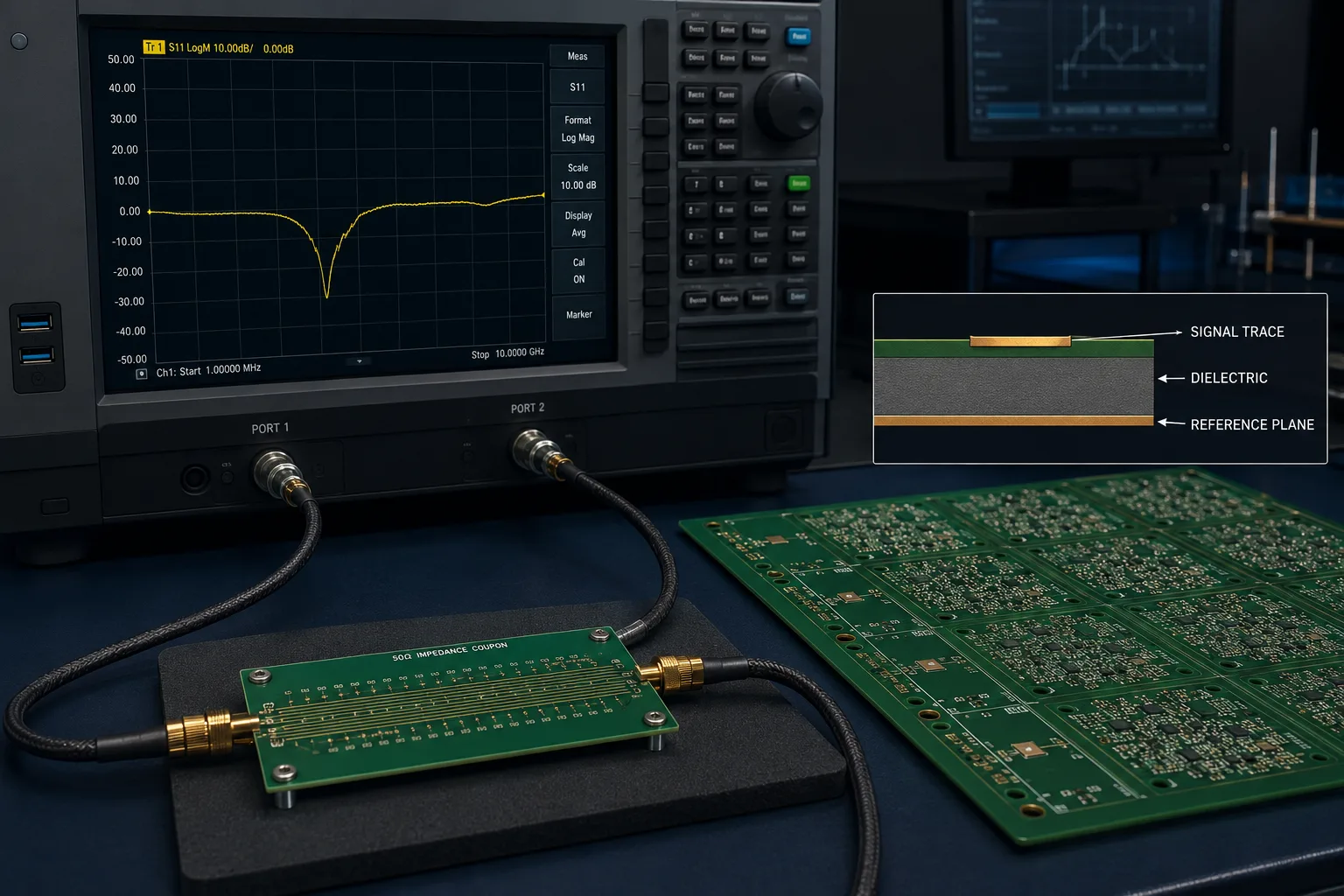
Impedance test coupons can be used to verify transmission-line characteristics during PCB fabrication.
A PCB manufacturer may use impedance testing methods to verify controlled-impedance structures.
A common approach is to use dedicated test coupons manufactured alongside the production PCB.
The coupon represents relevant PCB construction and transmission-line characteristics.
Testing can provide evidence that the fabricated structure meets the specified impedance requirements.
23. What Should Be Included in the Fabrication RFQ?
For a controlled-impedance PCB, the manufacturing RFQ should clearly communicate:
Electrical requirements
PCB construction
Geometry
Verification
This information allows the supplier to quote against a clear technical baseline.
24. Controlled Impedance Is a Collaboration
A successful impedance-controlled PCB requires coordination between several teams.
PCB Designer
Defines the electrical requirements and routing.
Signal-Integrity Engineer
Determines the transmission-line requirements where applicable.
Material/Stack-Up Engineer
Defines the physical construction.
PCB Fabricator
Evaluates manufacturability and process capability.
Quality Team
Verifies that the manufactured board meets requirements.
The strongest results occur when these activities are coordinated early.
25. Common Controlled-Impedance Design Mistakes
Mistake 1 — Treating impedance as only a trace-width problem
It is determined by the complete transmission-line geometry.
Mistake 2 — Designing before fixing the stack-up
Trace geometry can change when the stack-up changes.
Mistake 3 — Ignoring reference planes
Return-current paths are fundamental to high-speed signal behavior.
Mistake 4 — Changing trace geometry late
Last-minute routing changes can alter impedance.
Mistake 5 — Ignoring vias and connectors
Discontinuities can occur outside the straight PCB trace.
Mistake 6 — Assuming every supplier uses the same stack-up
Different constructions can produce different impedance results.
Mistake 7 — Not defining tolerance
A nominal impedance without an acceptable range may be ambiguous.
Mistake 8 — Treating simulation as fabrication verification
Calculated impedance and fabricated impedance are related but not identical.
26. Controlled Impedance Design Checklist
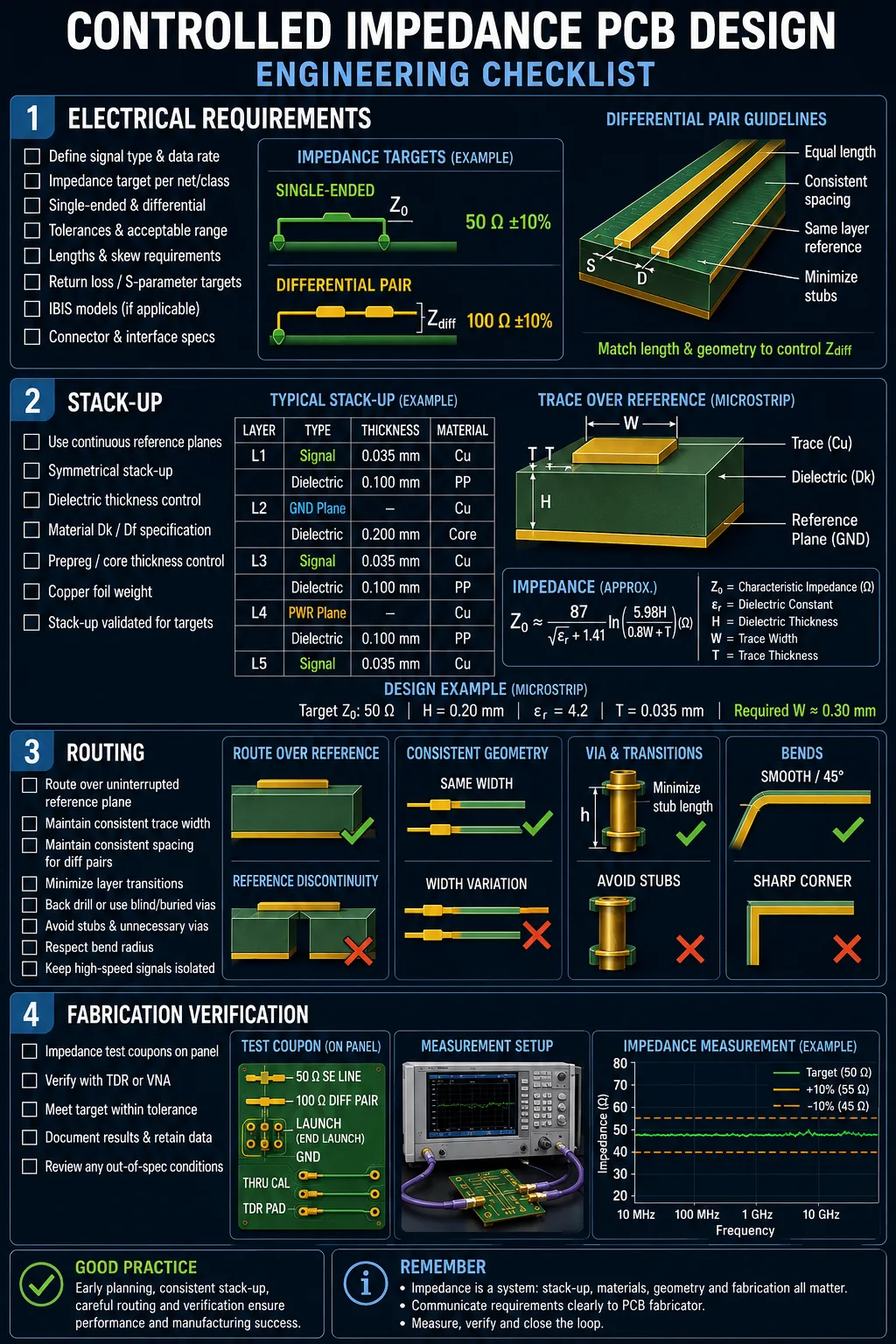
Controlled impedance should be reviewed across electrical design, stack-up, routing and manufacturing verification.
Before releasing the PCB for fabrication, verify:
Design
Stack-Up
Routing
Fabrication
27. Controlled Impedance and PCB Manufacturing Cost
Controlled impedance can affect manufacturing cost depending on the complexity of the requirement.
Potential cost drivers include:
However, the correct objective is not necessarily to minimize impedance-control cost.
It is to specify the appropriate performance requirement without over-engineering the PCB.
For example, unnecessarily tight impedance tolerances may add cost without delivering meaningful system-level benefit.
28. How Designers Can Make Impedance Control Easier to Manufacture
A few practical principles can help.
Establish the stack-up early
Avoid designing the complete PCB first and asking the manufacturer to solve impedance later.
Use practical geometries
Avoid unnecessarily extreme trace widths or spacings.
Maintain consistent reference planes
Give high-speed signals a predictable return path.
Minimize discontinuities
Review vias, connectors, pads and layer transitions.
Communicate clearly
Document impedance requirements in the fabrication package.
Engage the manufacturer early
Early feedback is usually easier and less expensive than late redesign.
29. Controlled Impedance Is About Repeatability
The goal is not simply to calculate:
50.0 Ω
once.
The manufacturing objective is to produce the PCB consistently within the required tolerance.
That means controlling the variables that influence the transmission line.
This is why PCB impedance control sits at the intersection of:
Electrical engineering + PCB design + materials + manufacturing process control.
30. Final Takeaway
Controlled impedance becomes increasingly important as signal transition times become faster and signal margins become tighter.
The fundamental principle is straightforward:
The impedance of a PCB transmission line is determined by its geometry and surrounding dielectric environment.
But achieving that impedance consistently requires more than selecting a trace width.
Designers need to consider:
Most importantly, controlled impedance should be treated as a design-to-manufacturing requirement—not just a PCB layout parameter.
When designers and fabricators establish the stack-up, geometry, tolerance and verification method together, the resulting PCB is much more likely to meet the intended signal-integrity requirements.
31. QUADRIONIX PERSPECTIVE
At QUADRIONIX, controlled-impedance PCB requirements are approached as a collaboration between engineering intent and manufacturing capability.
For high-speed and impedance-sensitive designs, the objective is not simply to manufacture a PCB with a specified trace width.
The objective is to ensure that:
→ Design requirements
→ Stack-up
→ Material
→ Trace geometry
→ Fabrication process
→ Verification
remain aligned.
This becomes particularly important when moving from prototype to repeat production, where manufacturing consistency matters as much as the initial design calculation.
If you have a Need to Manufacture an Impedance-Controlled PCB, Quadrionix team can assess the design from a fabrication and controlled-impedance perspective before production.
Design it right. Manufacture it consistently. Scale with confidence
Frequently Asked Questions
Ready to manufacture your electronics project?
Upload your Gerber files & BOM for automated DFM review, engineering feedback, and guaranteed delivery timelines.