Common PCB Assembly Issues and How to Avoid Them
Practical Guide to Identifying Assembly Defects, Understanding Root Causes, and Improving PCBA Manufacturing Yield
Introduction
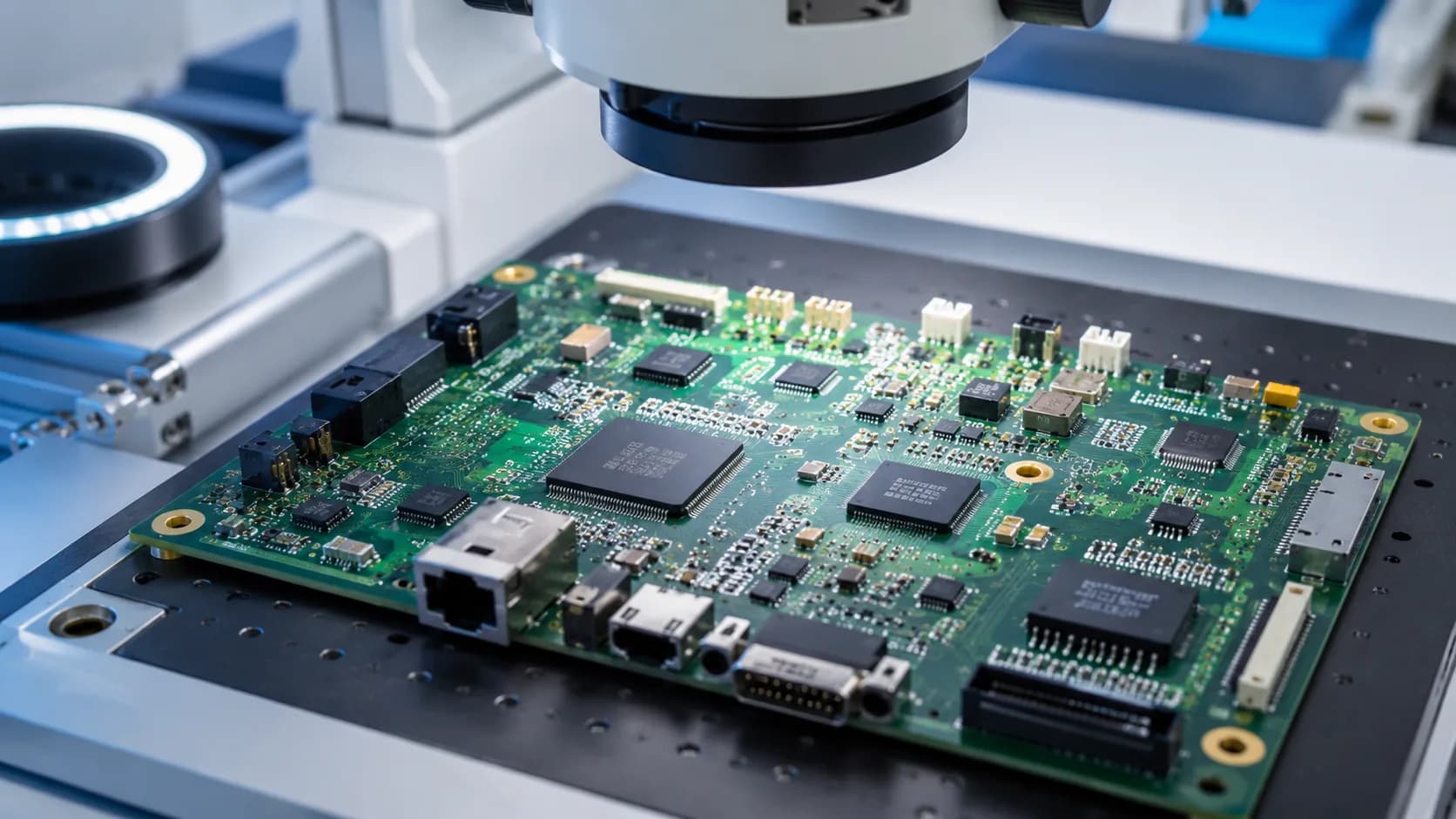
A PCB can be perfectly functional at the design stage and still encounter significant problems during assembly.
The transition from a bare PCB to a finished PCBA introduces a series of manufacturing processes—including solder-paste printing, component placement, reflow, through-hole soldering, inspection, cleaning where applicable, and functional testing. Each process introduces its own variables.
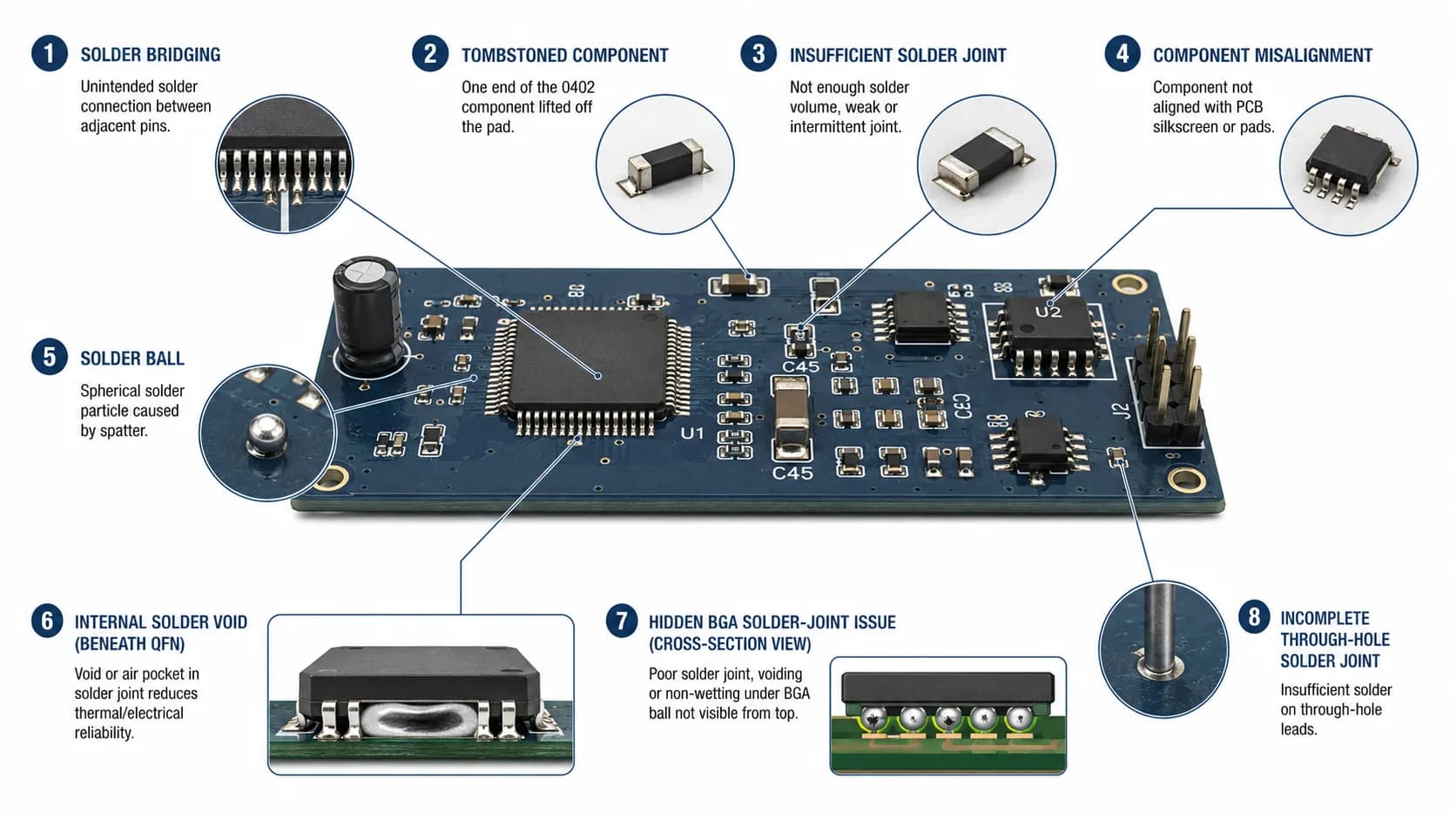
A defect may originate from the PCB design, component selection, solder-paste printing, stencil design, component placement, reflow profile, material condition, handling, or process control.
This is why PCB assembly quality should not be viewed simply as an inspection problem.
By the time a defect is detected at final inspection, the underlying cause may already have been introduced several process steps earlier.
A more effective approach is to understand the relationship between:
Design → Materials → Printing → Placement → Reflow → Inspection → Testing
and control the variables that influence each stage.
Industry standards provide an important framework for this process. IPC J-STD-001J addresses requirements for soldered electrical and electronic assemblies, while IPC-A-610J provides visual acceptability criteria for electronic assemblies.
1. Why PCB Assembly Defects Occur
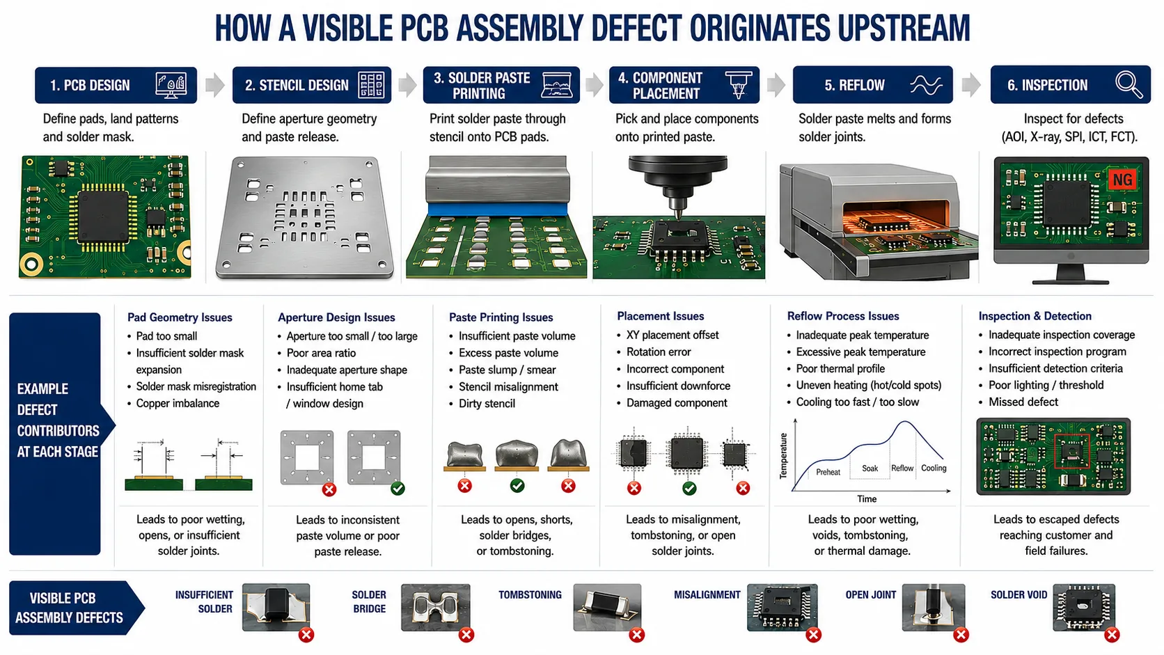
Most assembly defects do not have a single universal cause.
Consider a solder bridge between two fine-pitch pins.
Possible contributing factors include:
•
Excess solder-paste deposition
•
Stencil aperture design
•
Excessive paste spread
•
Pad geometry
•
Component placement accuracy
•
Board warpage
•
Printing alignment
•
Solder-paste condition
•
Reflow behaviour
Similarly, a tombstoned resistor may be associated with:
•
Unequal solder-paste volume
•
Pad geometry
•
Uneven heating
•
Component placement
•
PCB land design
•
Solder-paste deposition
This leads to an important principle:
The visible defect is not necessarily the root cause.
A good assembly process therefore uses root-cause analysis rather than simply repairing defective boards.
2. Solder Bridging
What Is Solder Bridging?
A solder bridge occurs when solder unintentionally connects two or more electrically separate conductors.
It is particularly problematic around:
•
Fine-pitch ICs
•
QFP packages
•
Connectors
•
Dense component areas
•
Small-pitch terminals
A bridge can create an electrical short circuit and may result in immediate functional failure or an intermittent field failure.
Common Causes
Typical contributors include:
•
Excess solder-paste volume
•
Incorrect stencil aperture dimensions
•
Poor print alignment
•
Excessive paste spread
•
Inadequate pad-to-pad spacing
•
Component placement issues
•
PCB or stencil contamination
•
Reflow-related solder movement
How to Prevent It
Prevention begins before the board reaches the SMT line.
Review:
•
PCB pad geometry
•
Component land pattern
•
Stencil aperture design
•
Paste volume
•
Printer alignment
•
Solder-paste condition
•
Reflow profile
•
Placement accuracy
Engineering takeaway: Don't simply reduce solder after a bridge is found. First determine whether the actual cause is Design → Stencil → Printing → Placement → Reflow.
3. Tombstoning
What Is Tombstoning?
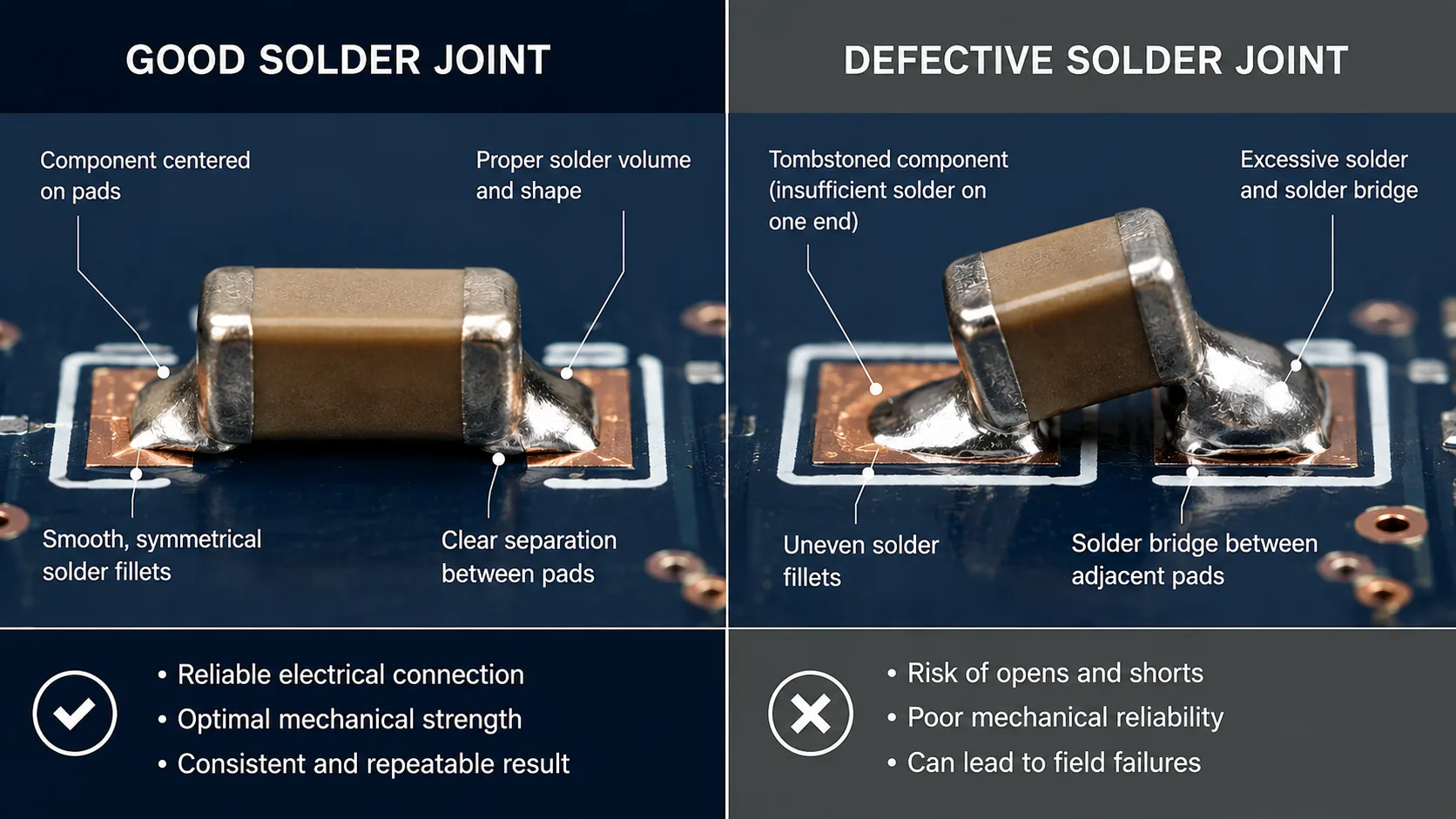
Tombstoning occurs when one end of a small surface-mount component lifts from the PCB during reflow, leaving the component standing at an angle.
It is particularly associated with:
•
Chip resistors
•
Chip capacitors
•
Small passive components
Why Does It Happen?
During reflow, solder on the two ends of the component should melt and exert relatively balanced forces.
If one side melts or wets significantly earlier than the other, the resulting surface-tension forces can lift one end of the component.
Potential contributors include:
•
Unequal solder-paste deposits
•
Unequal pad geometry
•
Uneven thermal exposure
•
Component placement offset
•
Differences in pad wetting
•
Stencil design
•
PCB layout asymmetry
How to Prevent Tombstoning
Check:
•
Pad symmetry
•
Stencil apertures
•
Paste volume balance
•
Component placement
•
Thermal profile
•
Land-pattern design
4. Insufficient Solder
What Is It?
An insufficient solder joint occurs when the solder volume or solder coverage does not provide the required connection.
Depending on the component and connection geometry, insufficient solder can affect:
•
Mechanical integrity
•
Electrical continuity
•
Thermal performance
•
Long-term reliability
Common Causes
•
Insufficient solder-paste volume
•
Incorrect stencil thickness
•
Blocked stencil apertures
•
Poor paste transfer
•
Incorrect aperture reduction
•
Pad contamination
•
Printing inconsistency
•
Component coplanarity issues
•
Incorrect process parameters
Prevention
Monitor:
Paste deposition → Paste volume → Placement → Reflow → Inspection
For critical assemblies, solder-paste inspection can provide valuable process feedback before boards proceed further through production.
5. Solder Opens
A solder open occurs when an intended electrical connection is not properly formed.
The component may appear physically present, but electrical continuity is missing.
Common causes include:
•
Missing solder paste
•
Insufficient solder
•
Poor wetting
•
Component placement problems
•
Pad contamination
•
Coplanarity problems
•
Incorrect stencil design
•
Component termination issues
For hidden solder joints such as BGAs, additional inspection methods may be required.
6. Component Misalignment
A component does not always need to be completely detached to cause a problem.
Excessive placement offset can affect:
•
Solder-joint geometry
•
Electrical clearance
•
Mechanical alignment
•
Connector engagement
•
Component-to-component clearance
•
Thermal behaviour
Common Causes
•
Pick-and-place calibration
•
Fiducial recognition problems
•
PCB warpage
•
Component package variation
•
Incorrect centroid data
•
Incorrect PCB land pattern
•
Excessive placement tolerance
Prevention
Good assembly preparation should include:
•
Correct centroid data
•
Verified component footprints
•
Accurate fiducials
•
Board-panelisation review
•
Placement-program verification
•
DFM/DFA review
7. Non-Wetting and Dewetting
What Is Non-Wetting?
Non-wetting occurs when molten solder does not properly spread and bond to the intended surface.
Instead of forming an appropriate solder connection, solder may remain partially separated from the pad or component termination.
Dewetting is different: solder initially wets the surface but subsequently pulls back, leaving areas of exposed substrate or an irregular solder coating.
Potential Causes
•
Surface contamination
•
Oxidation
•
Poor component termination
•
PCB surface-finish problems
•
Incorrect solder-paste condition
•
Inadequate thermal profile
•
Damaged component plating
•
Foreign material contamination
Prevention
Control:
•
PCB surface finish
•
Component termination quality
•
Storage conditions
•
Solder-paste handling
•
Board cleanliness
•
Reflow profile
•
Material traceability
8. Solder Balls
Small solder balls can appear around components after reflow.
Potential contributors include:
•
Solder-paste characteristics
•
Excess paste
•
Paste condition
•
Printing parameters
•
Reflow profile
•
Moisture
•
Component/PCB contamination
Prevention
Control:
•
Solder-paste storage
•
Paste age and handling
•
Printing parameters
•
Stencil design
•
Preheat and reflow conditions
•
PCB/component cleanliness
9. Voiding
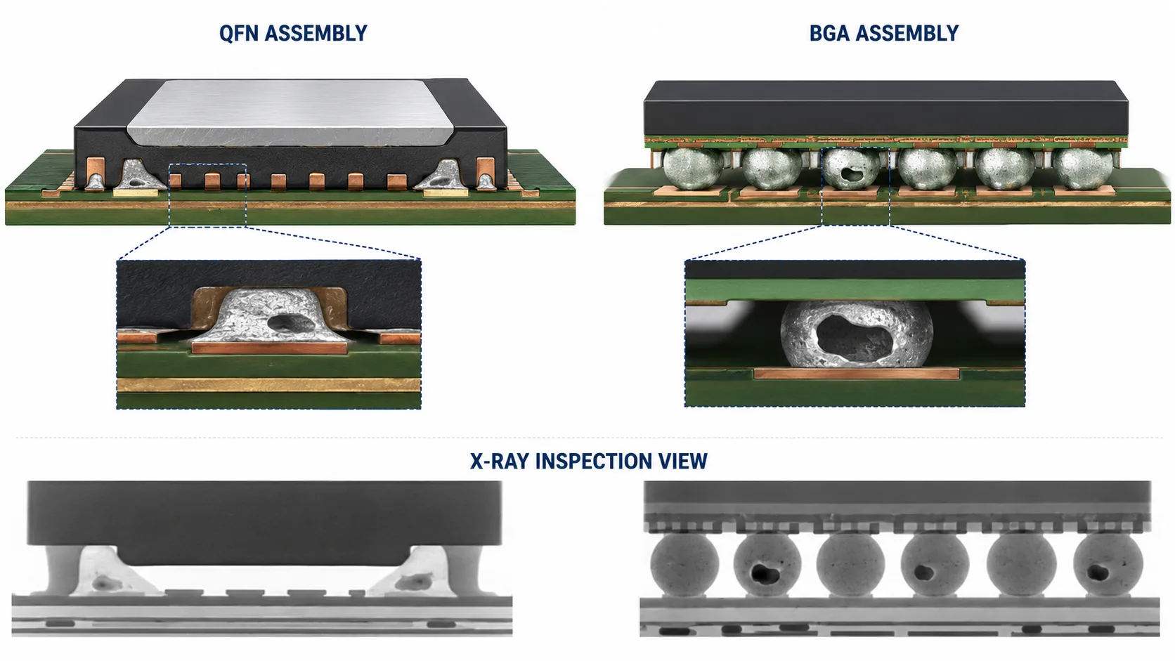
What Is Solder Voiding?
Voids are internal cavities within a solder joint.
They are not necessarily visible during normal optical inspection.
Voiding can be particularly important beneath:
•
QFN/BTC packages
•
Power components
•
Thermal pads
•
BGA structures
Why Can Voiding Matter?
For thermally important components, excessive voiding can interrupt portions of the thermal path.
It can also influence effective solder-joint area and reliability depending on the application and acceptance requirements.
How to Control It
Potential controls include:
•
Thermal-pad design
•
Stencil aperture pattern
•
Paste volume
•
Reflow profile
•
Solder-paste selection
•
Component design
•
PCB surface finish
For hidden joints, X-ray inspection may be appropriate.
10. BGA-Related Assembly Problems
BGA packages create a particular challenge because most solder joints are hidden beneath the component.
Common concerns include:
•
Insufficient solder
•
Voiding
•
Non-wetting
•
Open joints
•
Head-in-pillow
•
Component placement issues
These conditions may not be visible through conventional optical inspection.
Prevention
BGA assembly quality depends on several linked variables:
PCB design
↓
Land pattern
↓
Stencil design
↓
Paste deposition
↓
Component placement
↓
Reflow profile
↓
Inspection
A failure at any one stage can affect the final solder-joint quality.
11. Through-Hole Assembly Problems
PCB assembly isn't limited to SMT.
Through-hole components introduce their own manufacturing considerations.
Potential issues include:
•
Insufficient solder fill
•
Excessive solder
•
Poor wetting
•
Component lead positioning
•
Solder bridges
•
Incomplete barrel fill
•
Mechanical damage
•
Incorrect lead preparation
Through-hole requirements should be evaluated against the applicable product class and agreed acceptance criteria.
12. PCB Assembly Defects: Quick Reference
Assembly Issue | Typical Symptoms | Possible Causes | Prevention Focus |
|---|---|---|---|
Solder bridging | Solder connects adjacent pads | Excess paste, stencil, alignment, pad geometry | Stencil + print control |
Tombstoning | One end of passive component lifted | Unequal paste/thermal forces | Pad symmetry + paste balance |
Insufficient solder | Small or incomplete solder joint | Low paste volume, poor transfer | SPI + stencil/process control |
Solder open | Electrical connection absent | Missing/poor solder, wetting | Paste + placement + inspection |
Misalignment | Component shifted from pad | Placement/footprint/fiducial issues | CAD + centroid + placement |
Non-wetting | Solder fails to spread | Oxidation, contamination, plating | Material + surface control |
Solder balls | Small solder particles | Paste/reflow/printing conditions | Paste + process control |
Voiding | Internal cavities in solder joint | Trapped volatiles, design/process | Stencil + reflow + X-ray where required |
BGA defects | Hidden joint failure | Paste, placement, reflow | Process control + X-ray |
Through-hole solder defect | Incomplete or poor connection | Soldering/process/material issues | Process + inspection |
Note: This table is a troubleshooting guide, not an acceptance standard. Actual acceptance criteria should be defined by the applicable customer specification, product classification, drawing, purchase requirements and referenced standards.
13. Inspection: Finding Defects Before They Become Failures
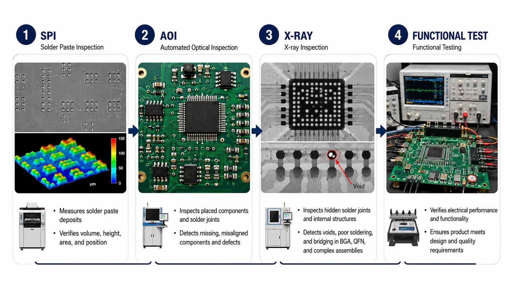
Inspection methods reveal different classes of problems.
SPI ( Solder Paste Inspection)
Evaluates solder-paste deposition before component placement and reflow.
Typical parameters include:
•
Paste volume
•
Height
•
Area
•
Position
•
Deposit consistency
AOI (Automated Optical Inspection)
Can inspect visible assembly characteristics such as:
•
Component presence
•
Component position
•
Polarity
•
Solder-related visual conditions
•
Missing components
•
Certain bridging conditions
X-Ray Inspection
Can help evaluate hidden solder joints and structures that cannot be inspected directly from the surface.
Applications include:
•
BGA joints
•
Bottom-terminated components
•
Hidden thermal pads
•
Voiding analysis
•
Certain through-hole structures
Functional Testing
Visual inspection cannot establish that the complete electronic assembly actually performs its intended function.
Depending on the product, testing may include:
•
Continuity testing
•
In-circuit test
•
Functional test
•
Programming
•
Communication-interface testing
•
Power-up verification
•
System-level testing
14. The Best Way to Prevent Assembly Defects
The strongest assembly strategy is not:
Build → Inspect → Repair
It is:
Design → Review → Control Process → Inspect → Test → Improve
This distinction matters.
A board with recurring defects may technically pass after manual rework, but that does not mean the manufacturing process is healthy.
A better question is:
Why did the defect occur in the first place?
That leads to process improvement rather than repeated repair.
15. Design for Assembly: Prevent Problems Before Production
Many assembly problems can be reduced during PCB design.
Before releasing a design, review:
Component Footprints
Are the land patterns appropriate for the actual component package?
Component Spacing
Is there sufficient clearance for placement, soldering, inspection and rework?
Fiducials
Are appropriate fiducials provided for machine vision and alignment?
Thermal Balance
Are large copper areas creating uneven thermal behaviour?
Fine-Pitch Devices
Are pad geometry and stencil requirements compatible with the assembly process?
BGA Devices
Has the escape routing, pad design and inspection strategy been considered?
Through-Hole Components
Are hole sizes, annular rings and assembly requirements appropriate?
Panelisation
Can the board be efficiently supported and processed through the assembly line?
This is why DFM/DFA review before manufacturing can be considerably more valuable than discovering problems after the first production run.
16. A Practical Pre-Production Assembly Checklist
Design
☐ Component footprints verified☐ Polarity/orientation verified☐ Fine-pitch clearances reviewed☐ BGA/QFN requirements reviewed☐ Thermal considerations reviewed☐ Fiducials included where required☐ PCB panelisation reviewed
BOM
☐ Manufacturer part numbers verified☐ Component availability checked☐ Lifecycle/obsolescence risks reviewed☐ Approved alternatives identified where appropriate☐ Package information verified
Manufacturing Data
☐ Gerber/ODB++/manufacturing data verified☐ Pick-and-place/centroid data verified☐ BOM matches placement data☐ Assembly drawing available☐ Revision numbers consistent
SMT Process
☐ Stencil design reviewed☐ Solder-paste specification defined☐ Reflow profile established☐ Placement program verified☐ SPI/AOI strategy defined
Inspection & Test
☐ Inspection criteria defined☐ X-ray requirement evaluated where applicable☐ Functional test requirements defined☐ Rework criteria established☐ Acceptance class documented
17. Representative Engineering Scenario
Fine-Pitch Controller Board
Consider a compact controller PCB containing:
•
A fine-pitch microcontroller
•
Multiple 0402 passives
•
A QFN power-management device
•
High-density connectors
•
Mixed SMT and through-hole components
During the first prototype build, several solder bridges appear around the fine-pitch device.
A simplistic response would be:
Reduce solder and rework the affected boards.
A better engineering investigation would examine:
PCB land pattern
↓
Stencil aperture geometry
↓
Paste deposition
↓
Printer alignment
↓
Component placement
↓
Reflow profile
↓
Inspection data
If SPI data shows excessive paste volume in the affected region, the problem may be upstream of the reflow process.
The corrective action could therefore involve stencil or printing optimisation rather than simply changing the reflow profile.
Good PCBA manufacturing controls the process that creates the defect—not merely the defect after it occurs.
18. What Procurement Teams Should Ask a PCBA Manufacturer
When evaluating a manufacturing partner, procurement teams often focus heavily on:
•
Unit price
•
MOQ
•
Lead time
•
Freight
•
Payment terms
Those are important—but they don't tell you whether the manufacturing process is capable of producing consistent assemblies.
Consider asking:
1. What assembly inspection processes are available?
Ask whether the manufacturer uses:
•
SPI
•
AOI
•
X-ray
•
Functional testing
as applicable to the project.
2. How are assembly defects recorded?
Look for evidence of structured defect tracking rather than informal rework.
3. How are first-article issues handled?
A capable manufacturer should have a defined process for identifying, documenting and correcting issues during prototype builds.
4. How are component substitutions controlled?
A substitute component should not simply be introduced because the original part is unavailable.
5. How is revision control handled?
The manufacturer should be able to demonstrate that the correct PCB, BOM and assembly data are being used.
6. What acceptance standard applies?
Ask:
What IPC class and customer-specific acceptance criteria will govern this build?
The applicable product classification and acceptance requirements should be established and documented before production.
19. IPC Standards: Where They Fit
Several IPC standards may be relevant to PCB assembly.
IPC J-STD-001
Requirements for soldered electrical and electronic assemblies, including materials, processes and acceptance requirements.
IPC-A-610
Visual acceptability criteria for electronic assemblies.
IPC-7351
Guidance related to land-pattern design for surface-mount components.
IPC-7711/7721
Rework, modification and repair practices.
Important
IPC standards should not simply be listed on a quotation as a marketing statement.
The applicable standard, revision, product class and customer-specific requirements should be agreed and documented before manufacturing.
20. From Defect Detection to Process Control
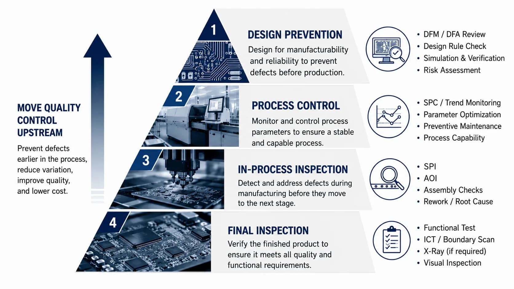
A mature manufacturing process progressively moves defect prevention upstream
Final Inspection Find defective boards after assembly -> In-Process Inspection Detect defects earlier through SPI/AOI/X-ray where appropriate -> Process Control Monitor printing, placement, reflow and material conditions -> Design Prevention Identify DFM/DFA risks before manufacturing begins.
The further upstream a problem is identified, the less expensive it generally is to correct.
21. QUADRIONIX Perspective
At QUADRIONIX, PCB assembly is not treated as simply placing components onto a fabricated board.
A reliable PCBA workflow connects:
→PCB Design
→ DFM/DFA Review
→ BOM Validation
→ PCB Fabrication
→ Solder-Paste Printing
→ Component Placement
→ Reflow / Through-Hole Processing
→ Inspection
→ Functional Validation
→ Production Readiness
The objective is to identify manufacturing risks as early as possible, establish appropriate inspection and process controls, and create a repeatable path from prototype to production.
For customers sourcing internationally, this becomes even more important because correcting an assembly problem after boards have crossed borders can introduce additional freight, lead-time, rework and schedule costs.
A technically sound manufacturing workflow therefore considers quality, manufacturability, supply continuity and logistics together.
22. Conclusion
PCB assembly defects rarely originate from a single isolated event.
A solder bridge may begin with stencil design.
A tombstoned capacitor may be influenced by pad geometry and thermal imbalance.
A non-wetted joint may originate from material or surface-condition problems.
A BGA defect may remain invisible until X-ray inspection.
And a recurring defect may indicate a process-control problem rather than an individual defective component.
The most effective approach is therefore systematic:
Design correctly.
Prepare manufacturing data carefully.
Control materials and processes.
Inspect at the appropriate stages.
Investigate root causes.
Validate the finished assembly.
Feed manufacturing learning back into design.
When these controls are connected, PCB assembly becomes more than a production step—it becomes an integrated part of product quality and manufacturing reliability.
Ready to manufacture your electronics project?
Upload your Gerber files & BOM for automated DFM review, engineering feedback, and guaranteed delivery timelines.