Trace Width and Spacing: What PCB Designers Need to Know
A Practical Guide to Current Capacity, Signal Integrity, Manufacturing Capability, Impedance, Clearance and PCB Reliability
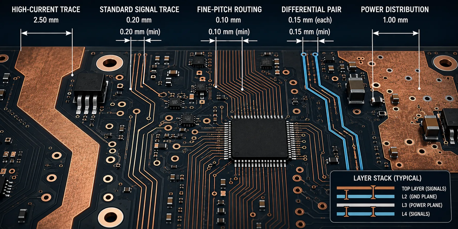
PCB trace width and spacing design showing high-current and signal-integrity routing
Trace width and spacing are two of the most fundamental parameters in PCB design.
They are also two of the easiest to oversimplify.
A common question is:
"What trace width should I use?"
Another is:
"What is the minimum spacing my PCB manufacturer can make?"
But a production-quality PCB cannot be designed around a single universal number.
Trace width can influence:
Trace spacing can influence:
And these parameters interact with other design variables including:
So the correct question is not:
"What is the standard PCB trace width?"
It is:
"What trace width and spacing are appropriate for this electrical requirement, PCB construction and manufacturing process?"
That distinction matters when a prototype must become a reliable production board.
1. What Is PCB Trace Width?
Trace width is the physical width of a copper conductor on the PCB.
For example:
0.15 mm
0.25 mm
0.50 mm
1.00 mm
2.00 mm
These are simply geometric dimensions.
But the electrical behavior of that trace depends on much more than width alone.
A 0.5 mm trace made using one copper thickness and PCB construction can behave very differently from a 0.5 mm trace using another copper thickness or routing environment.
For power traces, width is strongly associated with:
For high-speed traces, width becomes part of a larger transmission-line structure involving:
Therefore:
Trace width is an electrical and manufacturing design parameter—not merely a visual PCB layout parameter.
2. What Is PCB Trace Spacing?
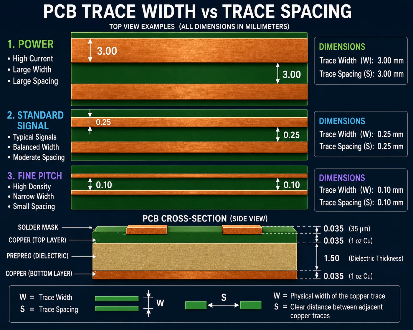
Trace width defines the conductor geometry; trace spacing defines the separation between adjacent conductive features. Both must be selected for electrical, reliability and manufacturing requirements.
Trace spacing is the distance between adjacent conductive features.
Depending on the context, this may mean the spacing between:
Spacing can affect both electrical performance and manufacturability.
For example, insufficient spacing can increase:
For high-voltage circuits, spacing can become a safety and reliability requirement rather than simply a routing preference.
3. Why There Is No Universal "Best" Trace Width
It is tempting to establish a company-wide rule such as:
"Use 0.2 mm traces everywhere."
That can simplify design-rule configuration, but it is not necessarily good engineering.
Consider three different nets:
A. Low-current digital signal
A relatively narrow trace may be completely adequate.
B. 5 A power rail
The same narrow trace may create excessive resistance and temperature rise.
C. High-speed controlled-impedance signal
Making the trace wider without considering the stack-up can alter impedance.
These three nets have fundamentally different requirements.
Therefore, trace dimensions should normally be determined net-by-net or by defined net classes, rather than treating the entire PCB identically.
4. The Main Factors That Determine Trace Width
Several variables should be considered when determining PCB trace width.
4.1 Current
Current is one of the most important factors for power traces.
As current increases, the designer generally needs to consider:
A trace carrying a few milliamps and a trace carrying several amperes should not automatically receive the same geometry.
4.2 Copper Thickness
Trace width cannot be evaluated independently of copper thickness.
A trace consists of a conductor with:
Width × Copper Thickness
forming its approximate cross-sectional area.
Increasing copper thickness can increase the current-carrying capability of a given trace geometry.
Common PCB copper constructions include different finished or base copper thicknesses depending on the fabrication requirement.
However, designers should be careful when using nominal copper values in calculations because PCB fabrication processes can affect the finished conductor geometry.
4.3 Allowable Temperature Rise
A PCB trace carrying current generates heat because of electrical resistance.
The designer therefore needs to define how much temperature rise is acceptable.
The acceptable temperature rise may depend on:
A trace designed for a high-temperature environment should not automatically use the same assumptions as a laboratory prototype operating under benign conditions.
4.4 Trace Length
Length affects resistance.
For a given conductor cross-section:
Longer trace → higher resistance
Higher resistance can produce:
This becomes particularly important for:
4.5 Temperature and Operating Environment
Ambient temperature matters.
A PCB operating inside a sealed enclosure in a high-temperature environment has less thermal margin than the same board operating in a well-ventilated laboratory.
Therefore, thermal design assumptions should reflect the actual product environment.
5. How Is PCB Trace Width Calculated for Current?
There is no single universal trace-width number because the calculation depends on the design assumptions.
A typical engineering approach starts by determining:
Industry-recognized PCB design guidance and calculators can then be used to estimate a suitable conductor width.
A useful conceptual relationship is:
Higher current + lower allowable temperature rise → larger required conductor cross-section
Similarly:
Higher copper thickness → potentially smaller width for the same current requirement
But these relationships should not be interpreted as permission to choose the smallest mathematically acceptable trace.
Manufacturing tolerance, reliability margin and thermal behavior also matter.
6. External vs Internal PCB Traces
The thermal environment of a trace depends partly on whether it is located on an external or internal layer.
External traces can exchange heat with the surrounding environment differently from internal traces embedded between dielectric layers.
Therefore, current-capacity calculations can distinguish between:
For multilayer boards, this distinction is important when routing power through internal layers.
A designer should not simply copy an external-layer trace-width rule onto an internal layer without considering the different thermal environment.
7. High-Current PCB Design Requires More Than a Wider Trace
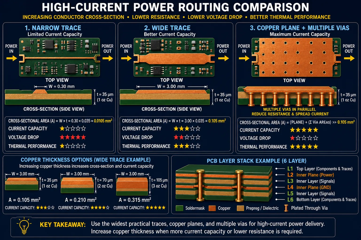
High-current PCB routing may use wider conductors, copper pours, planes, thicker copper or parallel current paths rather than simply increasing conventional trace width.
When current becomes significant, simply drawing a wider line is not always the best solution.
Other techniques may include:
For example, a high-current power path may use a copper polygon or plane instead of a conventional narrow trace.
This can reduce resistance and improve current distribution.
8. What Happens If a Power Trace Is Too Narrow?
An undersized power trace can create several problems.
Increased resistance
Higher resistance causes increased voltage drop.
Increased heating
Electrical power dissipated by a conductor is related to:
P = I²R
So as current increases, resistance becomes increasingly important.
Reduced system efficiency
Voltage and power losses can become significant in power-distribution paths.
Reliability concerns
Repeated thermal stress can contribute to long-term reliability problems.
For sensitive systems, voltage drop may also cause the load voltage to move outside its intended operating range.
Therefore, high-current trace design should consider the entire power path—not only the PCB trace width.
9. Trace Width and Voltage Drop
For a conductor:
V = I × R
and conductor resistance depends on:
Therefore, increasing trace width reduces resistance when other factors remain constant.
This matters particularly for:
For example, losing 100 mV on a 12 V rail may have little impact in one application but can be significant in a low-voltage high-current architecture.
10. Trace Spacing Is Not Just About Manufacturing
Trace spacing is often discussed as a minimum fabrication rule.
But it has at least three major dimensions:
a. Manufacturing clearance
Can the PCB fabricator reliably produce the intended geometry?
b. Electrical clearance
Can the conductors remain electrically isolated under the operating voltage and environmental conditions?
c. Signal integrity
Is the separation sufficient to control unwanted coupling and crosstalk?
These are different engineering questions.
A spacing that is perfectly manufacturable may not be appropriate for a high-voltage circuit.
Similarly, a spacing adequate for DC isolation may not provide the desired signal-integrity performance for high-speed signals.
11. Minimum Trace Spacing and PCB Fabrication
Every PCB fabrication process has practical limits for:
These limits can vary with:
Therefore, a designer should not design blindly around the smallest number found in a generic capability chart.
A more production-oriented approach is:
Design to a capability that the selected manufacturing process can reliably reproduce.
This becomes particularly important when moving from prototype to volume production.
12. Why Designing at the Absolute Minimum Is Usually a Poor Strategy
Suppose a manufacturer can theoretically fabricate a particular very narrow trace and very small spacing.
That does not necessarily mean the design should use those limits everywhere.
Designing with excessive dependence on minimum capability can reduce manufacturing margin.
A slightly more relaxed design may provide:
This is one of the key principles of Design for Manufacturability (DFM).
13. Trace Width and Spacing in Fine-Pitch Designs
Modern electronics increasingly use:
These packages can force routing into very small spaces.
The designer may need to balance:
Package escape routing
against
manufacturing capability
against
signal integrity
against
reliability
A design that looks perfectly routable inside the CAD tool may still require careful fabrication review.
This is where early DFM interaction with the PCB manufacturer can be valuable.
14. Trace Spacing and Crosstalk
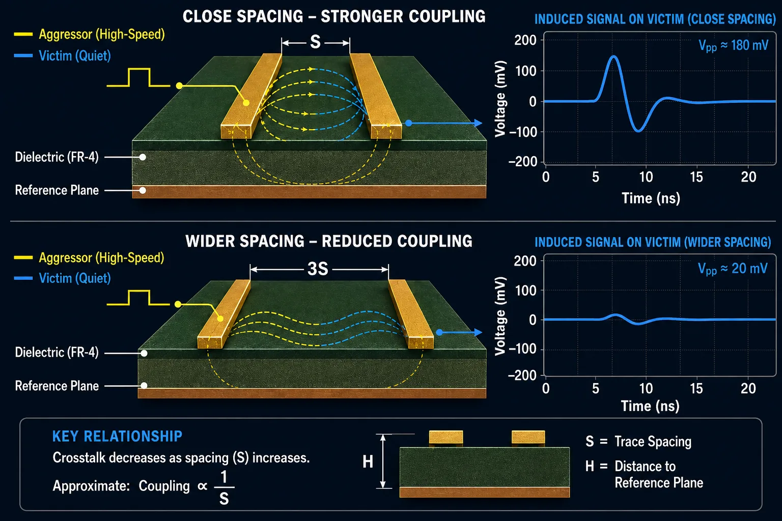
Reducing the spacing between parallel high-speed traces can increase coupling and crosstalk; the required spacing depends on the interface and stack-up.
When two signal traces run close to one another, electromagnetic coupling can occur.
The amount of coupling depends on several factors, including:
A simple rule such as "keep all traces 3W apart" can be useful as a design heuristic in some contexts, but it should not be treated as a universal signal-integrity law.
For fast signals, rise time can be more important than the nominal clock frequency when evaluating whether transmission-line and crosstalk effects matter.
That is why high-speed PCB routing should be based on the actual electrical behavior of the interface rather than relying solely on generic spacing rules.
15. Controlled Impedance Changes the Trace-Width Question
For controlled-impedance designs, the question is no longer:
"How wide should my trace be?"
It becomes:
"What trace geometry produces the required impedance in this PCB stack-up?"
For a microstrip or stripline structure, impedance is influenced by factors including:
For differential pairs, the spacing between the two conductors also affects differential impedance.
Therefore, a designer cannot reliably choose a trace width from a generic table without considering the actual stack-up.
16. Differential Pair Width and Spacing
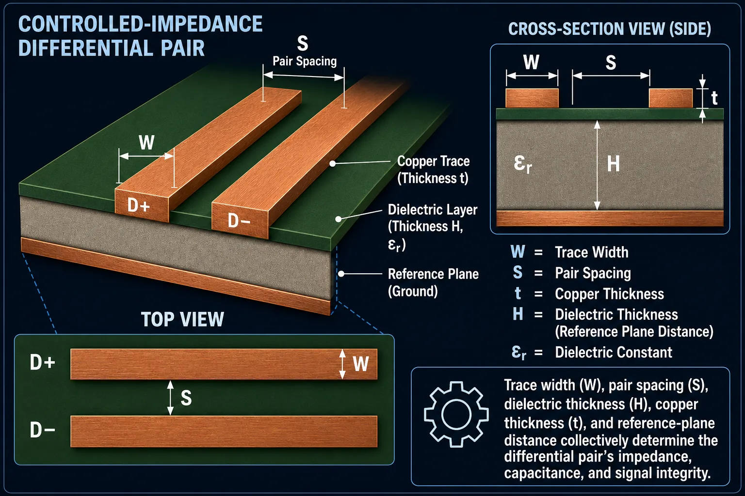
For controlled-impedance differential routing, trace width and pair spacing must be considered together with the PCB stack-up.
Differential interfaces such as high-speed serial links use two related conductors.
The design must consider:
Changing either the width or spacing can alter the differential impedance.
This is why controlled-impedance differential routing should be developed together with the PCB stack-up.
17. Trace Width Is Also a Thermal Design Parameter
Trace width is frequently treated as an electrical parameter.
It is also a thermal parameter.
A conductor dissipates heat according to its electrical resistance and current.
A wider conductor generally provides:
Thermal design should also consider nearby:
For high-power PCBs, the trace should be considered as part of the complete thermal architecture.
18. Copper Pours and Planes Can Change the Design Strategy
Instead of routing a high-current net as an individual trace, a designer can sometimes use:
These approaches can provide a larger copper cross-sectional area and lower resistance.
However, copper pours also need proper consideration of:
A large copper region is not automatically a better PCB design.
19. Trace Spacing Around High-Voltage Nets
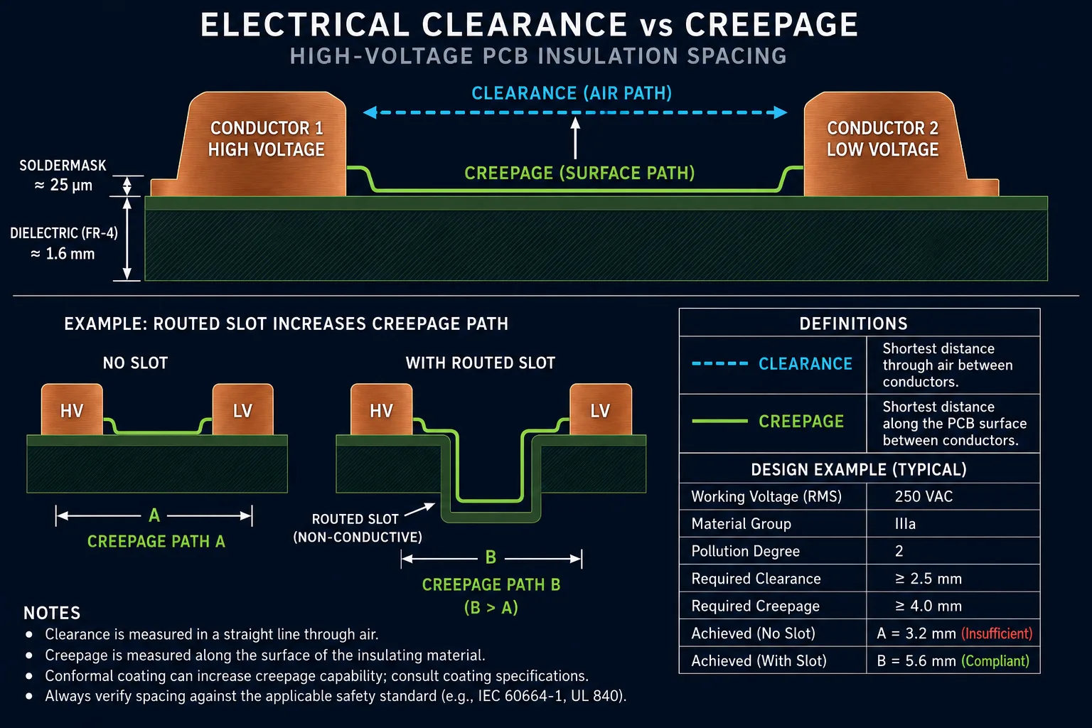
Clearance is measured through air, while creepage follows the insulating surface between conductive parts; high-voltage PCB requirements must be established from the applicable safety requirements.
High-voltage PCB design introduces a different set of requirements.
The designer may need to consider:
Clearance
Clearance is generally the shortest distance through air between conductive parts.
Creepage
Creepage is the shortest distance along the surface of an insulating material between conductive parts.
These should not be treated as interchangeable.
For safety-critical or mains-connected designs, trace spacing should be established according to the applicable product and safety requirements rather than a generic PCB fabrication minimum.
20. Trace Width Around Vias and Pads
A common mistake is to calculate an adequate trace width but overlook the current path through:
For a high-current net, the narrowest section can become the limiting point.
Consider a power path:
Connector → Wide Trace → Via → Internal Plane → Via → Wide Trace
If the vias or neck-down regions cannot carry the required current or create unacceptable thermal stress, increasing the width of the horizontal trace does not solve the complete problem.
Therefore:
Always evaluate the complete current path, not only the longest copper trace.
21. Avoid Unnecessary Neck-Downs
High-current routing frequently becomes narrower around:
Some neck-down is unavoidable.
But unnecessary narrowing should be avoided.
For example:
Wide copper → narrow section → wide copper
creates a localized resistance and thermal bottleneck.
When designing power paths, identify the narrowest section and evaluate whether it is acceptable.
22. Trace Width and Manufacturing Tolerances
The width specified in CAD is not necessarily identical to the final measured copper geometry.
Manufacturing processes introduce tolerances.
Factors can include:
This is particularly important when trace width approaches the fabrication capability limit.
A design with generous geometry has more manufacturing margin than one that depends on extremely tight dimensional control.
23. Why Trace Width and Spacing Should Be Defined as Design Rules
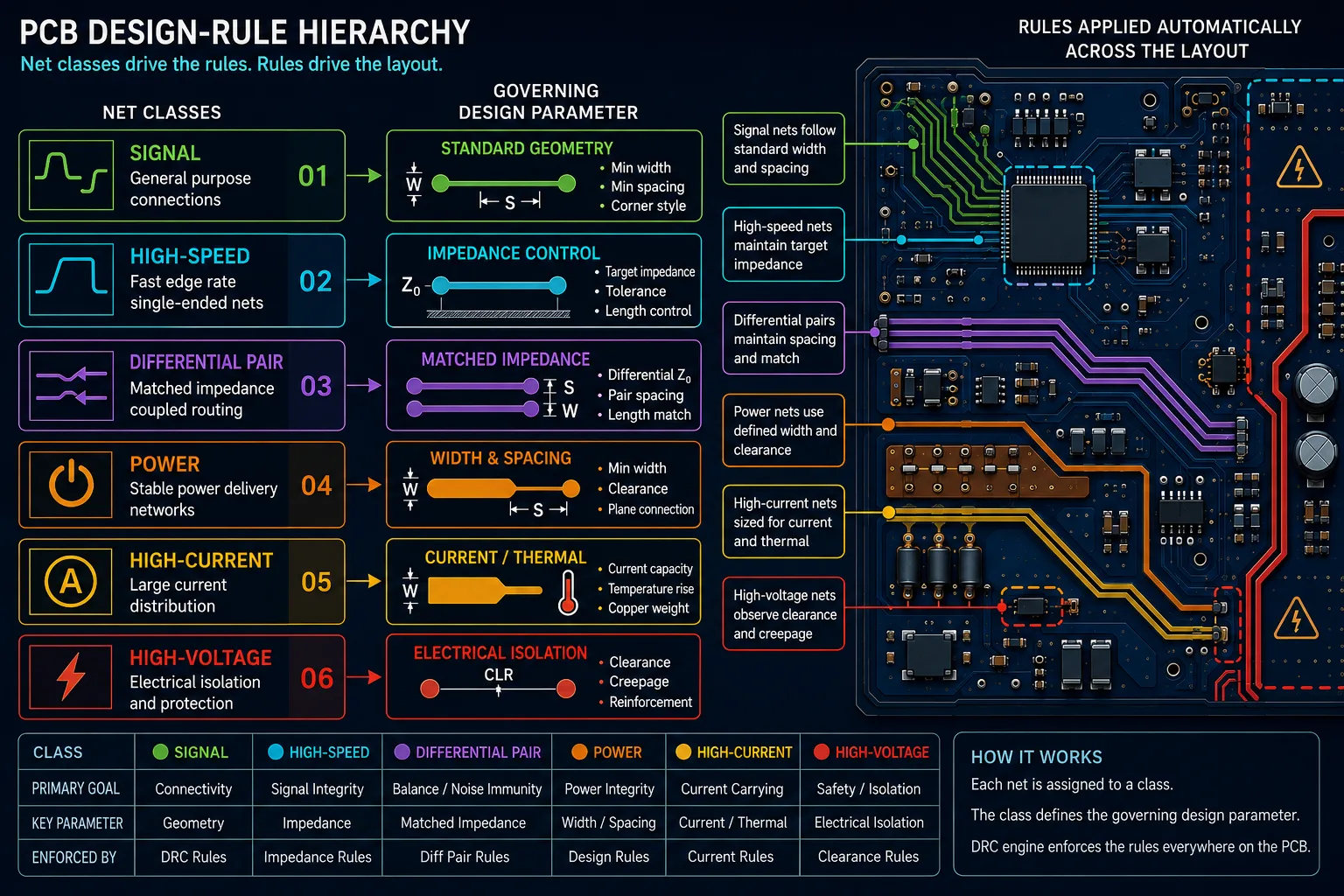
Defining trace-width and spacing rules by net class helps maintain consistent electrical and manufacturing constraints throughout the PCB layout.
For production PCB design, manually deciding trace width every time is inefficient and error-prone.
Modern PCB CAD tools allow designers to define design rules and net classes.
For example:
| Net Class | Typical Application | Width Strategy |
|---|---|---|
| Signal | Low-speed digital/control | Standard routing width |
| High-Speed | Fast digital interfaces | Stack-up/impedance-driven |
| Differential | High-speed differential interfaces | Width + pair spacing |
| Power | Moderate current | Current/thermal-driven |
| High Current | Power distribution | Larger copper geometry |
| High Voltage | Isolation-critical nets | Clearance/creepage-driven |
The exact values should be determined from the electrical and manufacturing requirements of the project.
This approach makes the design more consistent and easier to review.
24. A Practical Trace Width Selection Workflow
Instead of beginning with a preferred trace width, use a requirement-driven process.
Step 1 — Identify the net
Is it:
Step 2 — Determine the electrical requirement
Identify:
Step 3 — Determine the PCB construction
Confirm:
Step 4 — Determine thermal requirements
Consider:
Step 5 — Determine manufacturing capability
Confirm:
Step 6 — Apply design margin
Avoid unnecessarily designing directly at the manufacturing limit.
Step 7 — Validate the complete routing
Check:
This produces a much more defensible design than selecting a universal trace width.
25. Example: Why One PCB May Need Several Trace Widths
Consider a hypothetical controller board containing:
Microcontroller GPIO
Low-current digital signal.
→ Relatively modest trace geometry may be sufficient.
High-speed communication interface
Signal integrity becomes important.
→ Width and spacing may need to be controlled against the stack-up.
3.3 V power rail
Moderate current.
→ Voltage drop and thermal considerations matter.
Motor supply
High current.
→ Wider copper, planes or multiple parallel paths may be required.
Mains input
High voltage.
→ Clearance and creepage requirements become critical.
One PCB can therefore contain multiple trace-width and spacing rules simultaneously.
That is normal engineering practice.
26. Common Trace Width and Spacing Mistakes
Mistake 1 — Using one width for every net
Why it fails:Different electrical functions have different requirements.
Mistake 2 — Choosing width only from current
Why it fails:High-speed and controlled-impedance traces have additional constraints.
Mistake 3 — Using the smallest manufacturer capability everywhere
Why it fails:Minimum capability is not necessarily the best production design target.
Mistake 4 — Ignoring copper thickness
Why it fails:Conductor cross-section depends on both width and copper thickness.
Mistake 5 — Ignoring voltage drop
Why it fails:A trace can survive thermally while still producing unacceptable voltage loss.
Mistake 6 — Ignoring vias
Why it fails:The via or neck-down may become the bottleneck.
Mistake 7 — Treating all high-speed traces as ordinary signals
Why it fails:Rise time, impedance, return path and crosstalk can become important.
Mistake 8 — Confusing clearance with creepage
Why it fails:They represent different physical paths and can have different safety implications.
Mistake 9 — Checking only the CAD view
Why it fails:The final manufacturing geometry and fabrication constraints still need verification.
Mistake 10 — Designing without considering the manufacturer's process
Why it fails:A technically routable design may still be unnecessarily difficult or risky to fabricate.
27. How Trace Width and Spacing Affect PCB Cost
Trace width and spacing can indirectly influence manufacturing cost.
Very dense designs may require:
A board designed comfortably within a standard fabrication capability can be easier and more economical to manufacture than one that continuously pushes process limits.
This is especially relevant when optimizing a PCB for volume production.
The goal should therefore not be:
"How small can I make the traces?"
but:
"What is the smallest geometry I actually need for this design?"
That is a much better manufacturing question.
28. What Engineers Should Give Their PCB Manufacturer
When requesting fabrication, the manufacturer should have enough information to understand the intended PCB construction and performance requirements.
Depending on the design, this can include:
For high-current designs, communicating current-critical regions can also help during engineering review.
For high-speed designs, identifying impedance-controlled interfaces is particularly useful.
29. What Should a PCB Manufacturer Review?
A competent manufacturing review should go beyond simply asking:
"Are the files present?"
The engineering review should consider whether the intended design is compatible with the selected manufacturing process.
Areas may include:
Geometry
Stack-up
Electrical requirements
Manufacturing
Reliability
This is where DFM becomes valuable.
30. Trace Width and Spacing: Engineer's Quick Reference
| Design Requirement | Primary Consideration |
|---|---|
| Low-current signal | Manufacturing capability |
| High-current power | Current, temperature rise, voltage drop |
| Long power trace | Resistance and voltage drop |
| High-speed signal | Impedance, return path, crosstalk |
| Differential pair | Differential impedance and pair geometry |
| High-voltage net | Clearance, creepage and applicable safety requirements |
| Fine-pitch package | Escape routing and fabrication capability |
| Internal power layer | Thermal behavior and copper structure |
| High-density PCB | Manufacturing tolerance and process capability |
| Production volume | Manufacturing margin and repeatability |
31. A Practical PCB Trace Width & Spacing Checklist
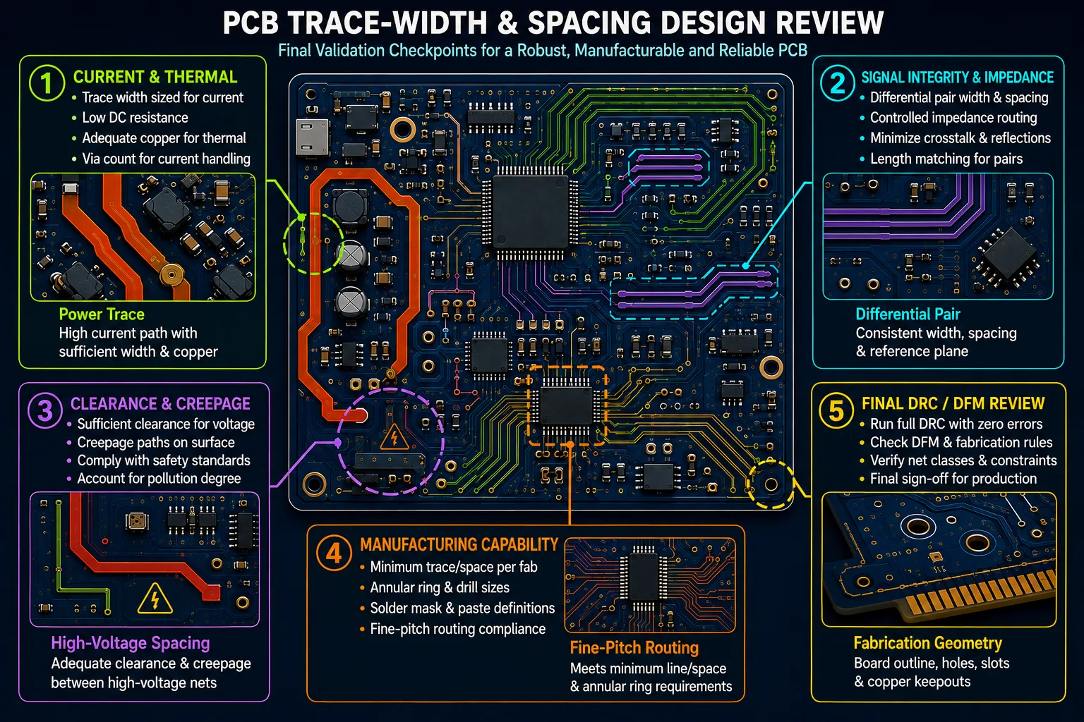
Trace width and spacing should be validated against electrical, thermal, safety, signal-integrity and manufacturing requirements before production release.
Before releasing a PCB design for manufacturing, ask:
Electrical
PCB Construction
Manufacturing
High-Current Paths
High-Voltage Paths
Final Review
32. The Key Principle: Design for the Complete System
Trace width and spacing should never be considered in isolation.
For a production PCB, the designer needs to connect several disciplines:
Electrical Requirements
↓
PCB Stack-Up
↓
Trace Geometry
↓
Thermal Behavior
↓
Signal Integrity
↓
Manufacturing Capability
↓
Reliability
This is why a trace that looks "correct" in a PCB layout may still require engineering review.
33. Final Takeaway
There is no single correct PCB trace width or spacing value that applies to every design.
The right geometry depends on what the conductor is doing.
For power traces, consider:
Current + copper thickness + temperature rise + resistance + voltage drop
For high-speed traces, consider:
Trace geometry + dielectric structure + reference plane + impedance + return path + crosstalk
For high-voltage circuits, consider:
Clearance + creepage + working voltage + applicable safety requirements
For manufacturing, consider:
Minimum capability + process tolerance + manufacturing margin + production repeatability
And across all of them:
Do not design only to what a manufacturer can theoretically fabricate. Design to what can be fabricated reliably and repeatedly for the intended product.
That is the difference between a PCB that merely passes DRC and a PCB that is engineered for production.
34. Conclusion
Trace width and spacing decisions are most effective when they are considered before the PCB is released for fabrication, rather than discovered as manufacturing issues later.
A structured engineering review can evaluate:
For complex or production-critical PCB designs, involving the manufacturing partner early can help identify issues before they become fabrication or NPI problems.
Frequently Asked Questions
Ready to manufacture your electronics project?
Upload your Gerber files & BOM for automated DFM review, engineering feedback, and guaranteed delivery timelines.