Stencil Design and Its Impact on SMT Assembly
How stencil thickness, aperture design, solder-paste deposition and printing controls influence SMT quality, yield and PCB assembly reliability
Stencil Design and Its Impact on SMT Assembly
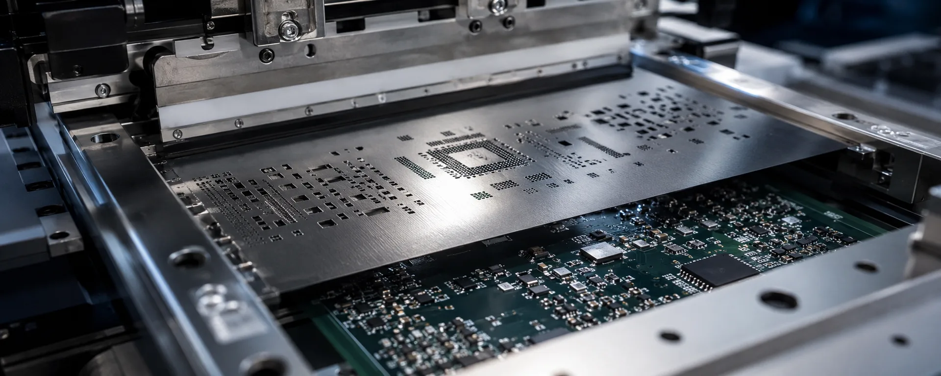
Precision SMT stencil depositing solder paste onto a PCB during assembly
In SMT manufacturing, one of the most important steps happens before a component is placed on the PCB.
It is the deposition of solder paste.
The solder paste must be applied to the correct pads, in the correct location, and in an appropriate volume.
Too little solder paste can contribute to:
Too much can increase the risk of:
The tool responsible for controlling this deposition is the SMT stencil.
A stencil may appear to be a relatively simple sheet of metal with openings.
In reality, stencil design is a critical part of the SMT process.
The stencil connects:
PCB design → solder-paste deposition → component placement → reflow → solder-joint quality
A well-designed stencil can improve process stability and yield.
A poorly designed stencil can create defects before the PCB even reaches the reflow oven.
1. What Is an SMT Stencil?
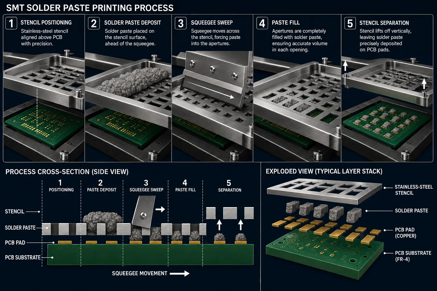
The SMT stencil controls where solder paste is deposited and strongly influences solder-joint formation later in the process.
An SMT stencil is a precision sheet, commonly made from stainless steel, containing openings known as apertures.
During solder-paste printing, the stencil is aligned with the PCB.
Solder paste is deposited across the stencil using a squeegee or automated printing system.
The paste passes through the apertures and is deposited onto the PCB pads.
The stencil is then separated from the PCB, leaving controlled deposits of solder paste.
The basic process is:
→ Stencil alignment
→ Paste application
→ Squeegee movement
→ Aperture filling
→ Stencil separation
→ Solder-paste deposits on PCB pads
The quality of these deposits directly affects downstream assembly.
2. Why Stencil Design Matters
Stencil design determines the amount and location of solder paste deposited onto each PCB pad.
That makes it one of the first major process controls in SMT assembly.
A good stencil must balance the requirements of very different components on the same PCB.
For example, a board may contain:
These components do not necessarily require the same solder-paste volume.
Therefore, one simple aperture strategy may not be optimal for the entire board.
3. Stencil Thickness
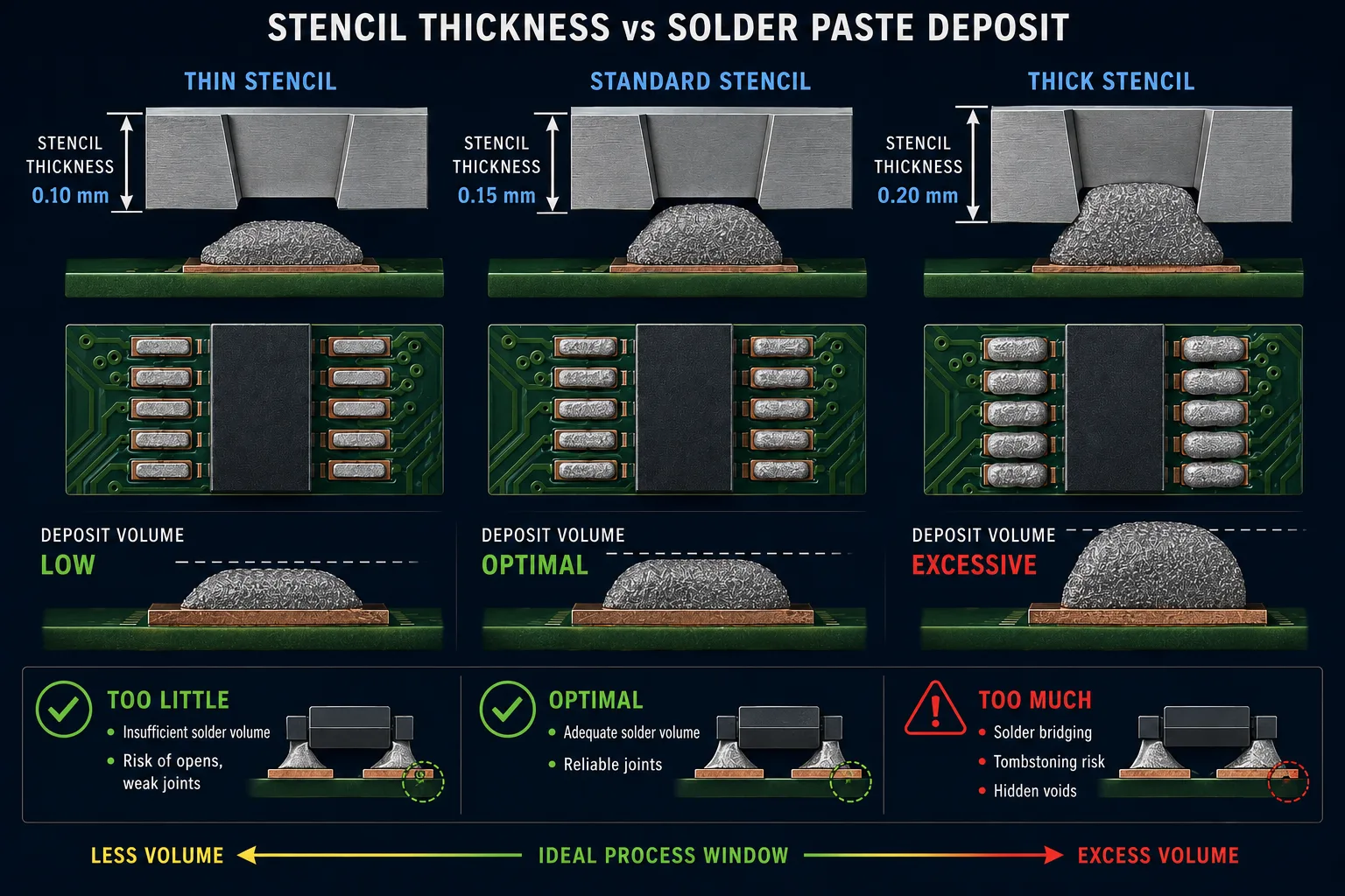
Stencil thickness influences solder-paste volume and must be selected according to the component mix and manufacturing requirements.
One of the most important stencil parameters is thickness.
A thicker stencil generally allows more solder paste to be deposited.
A thinner stencil generally deposits less.
But choosing thickness is not simply a matter of:
"More solder is better."
The stencil needs to support the smallest components while still providing enough solder for larger components and special features.
For example:
Very fine-pitch components
may require careful control of paste volume to reduce bridging.
Meanwhile:
Large thermal pads
may require substantially more solder volume.
This creates a balancing problem.
4. Aperture Design
The openings in the stencil are called apertures.
Their:
determine the solder-paste deposit.
Aperture design is therefore just as important as stencil thickness.
For a simple rectangular PCB pad, the aperture may closely follow the pad shape.
For more demanding components, the aperture may need to be modified.
Examples include:
5. Aperture Reduction
In some cases, the aperture may intentionally be made smaller than the corresponding PCB pad.
This is known as aperture reduction.
The objective may be to control solder volume or reduce the likelihood of solder bridging.
The exact reduction should be determined from:
It should not be applied blindly to every component.
6. Area Ratio
One of the important concepts in stencil design is the area ratio.
It helps describe how effectively solder paste can transfer through an aperture.
For a simplified rectangular aperture, area ratio can be expressed as:
Area Ratio = Aperture opening area ÷ Aperture wall area
For a rectangular aperture with width W, length L, and stencil thickness T:
Area Ratio = (W × L) / [2T(W + L)]
A commonly used guideline for paste-transfer performance is an area ratio around 0.66 or greater, although actual process capability depends on stencil technology, paste, aperture geometry and manufacturing conditions.
The important concept is:
As apertures become smaller relative to stencil thickness, reliable paste transfer becomes more challenging.
7. Aspect Ratio
Another useful concept is the aspect ratio.
For a rectangular aperture:
Aspect Ratio = Aperture width ÷ Stencil thickness
Like area ratio, it helps indicate whether solder paste can release effectively from the aperture.
Modern stencil design should consider both the geometry of the opening and the stencil thickness rather than looking only at the PCB pad dimensions.
8. Why Fine-Pitch Components Are Challenging
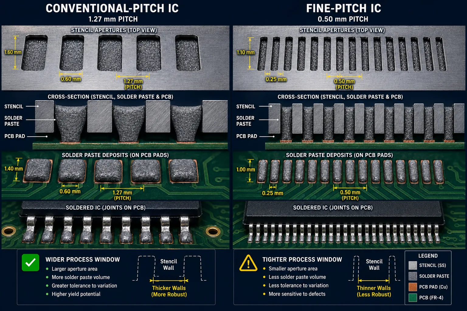
Fine-pitch components require tighter control of aperture geometry and solder-paste deposition.
As component pitch decreases, the distance between adjacent solder deposits becomes smaller.
That creates a narrower process window.
A small printing variation can potentially result in:
This is why fine-pitch components often require careful aperture optimization.
9. BGA Stencil Design
BGA packages are especially sensitive to stencil design because they contain an array of closely spaced solder joints.
The stencil must provide consistent solder-paste deposition across the entire BGA footprint.
Potential considerations include:
A small variation across hundreds of BGA pads can create significant assembly risk.
This is why BGA stencil design should be reviewed as part of the overall BGA assembly process.
10. QFN and Thermal Pad Design
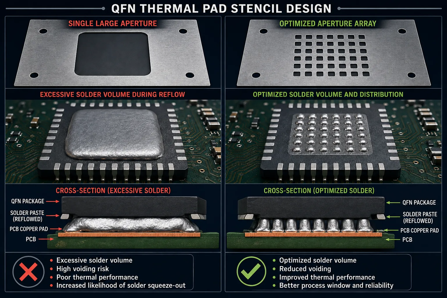
Dividing large thermal-pad apertures can help control solder volume and improve assembly behavior.
QFN packages often contain a large central exposed pad.
Applying a single large stencil opening over that pad can result in excessive solder volume.
During reflow, excessive solder can cause the component to rise or tilt.
A common approach is to divide the thermal-pad stencil opening into several smaller apertures.
This can help control:
The exact aperture pattern should be determined according to the component and process requirements.
11. Stepped Stencils
Some PCBs contain a mixture of very small and very large components.
Using one uniform stencil thickness can create a compromise.
A stepped stencil can use different thicknesses in different regions.
For example:
Thin region
→ Fine-pitch components
Thicker region
→ Large components requiring greater solder volume
This can provide more flexibility when a PCB contains widely varying component geometries.
However, stepped stencils add complexity and should be justified by the assembly requirements.
12. Stencil Material
Stencils are commonly manufactured from stainless steel because it provides:
For demanding applications, the manufacturing quality of the stencil itself matters.
Factors include:
A theoretically good aperture design can still perform poorly if the stencil is manufactured poorly.
13. Electroformed vs Laser-Cut Stencils
Different stencil manufacturing technologies can be used depending on the application.
Laser-cut
Widely used and capable of producing precise apertures.
Electroformed
Can provide very smooth aperture walls and may be considered for demanding fine-pitch applications.
The choice depends on:
14. Stencil Alignment
Even a well-designed stencil will not produce good results if it is incorrectly aligned with the PCB.
Modern SMT printers use alignment systems to position the stencil accurately relative to the board.
Important factors include:
Good alignment helps ensure that solder paste lands where it is intended.
15. PCB Support During Printing
The PCB should be adequately supported during stencil printing.
A board that flexes or moves during printing can affect paste transfer.
Support methods can include:
The appropriate solution depends on the PCB geometry and production equipment.
Large or thin boards may require particular attention.
16. Solder Paste Selection
Stencil design cannot be considered independently from solder paste.
Paste characteristics such as:
can affect the printing process.
Fine-pitch applications may require solder paste with characteristics appropriate for the component geometry and stencil apertures.
The objective is a stable and repeatable printing process.
17. Stencil Printing Parameters
Even the right stencil can produce poor results if the printing process is poorly controlled.
Important parameters include:
These parameters should be established through process development rather than arbitrary settings.
18. Stencil Cleaning
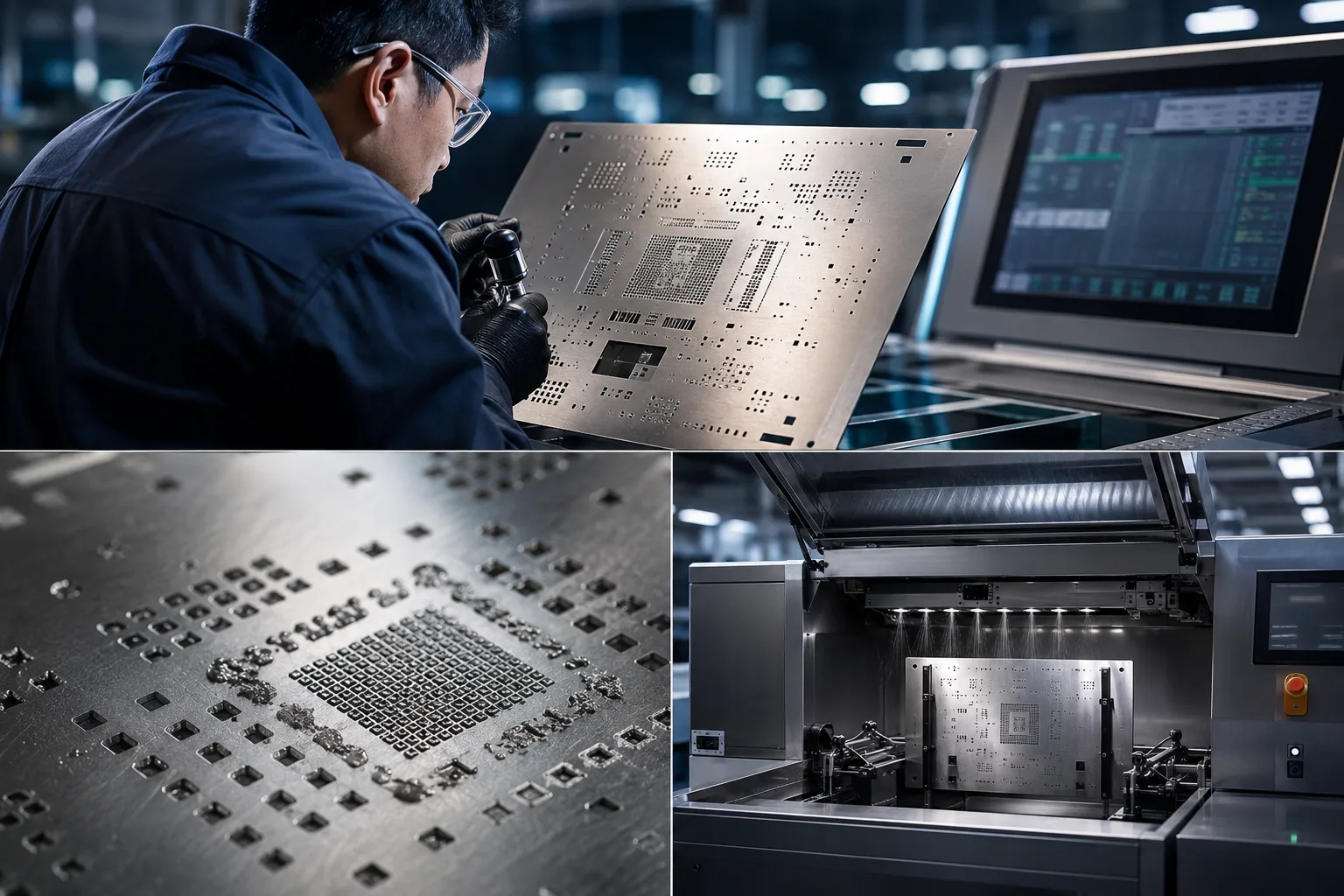
Stencil condition and cleanliness directly influence the consistency of solder-paste transfer.
Solder paste residue can accumulate around stencil apertures during production.
If not controlled, this can affect paste transfer.
Stencil cleaning may therefore be performed at defined intervals or triggered by process monitoring.
The cleaning method should be compatible with:
Fine-pitch apertures can be particularly sensitive to contamination.
19. SPI: Measuring What the Stencil Deposited
Solder Paste Inspection (SPI) provides an important feedback mechanism after printing.
SPI can evaluate characteristics such as:
This allows the manufacturing team to determine whether the stencil and printing process are producing the intended deposits.
Instead of discovering a solder defect after reflow, the process can potentially identify a printing problem earlier.
20. Why SPI and Stencil Design Work Together

SPI data can be used to validate solder-paste deposition and continuously improve the stencil printing process.
Consider a board with repeated insufficient paste deposits.
SPI may identify the pattern.
The manufacturing team can then investigate:
→ Stencil aperture
→ Paste
→ Printing parameters
→ Stencil condition
→ PCB support
This makes SPI more than an inspection tool.
It can become part of a closed-loop process-control strategy.
21. Common Stencil-Related SMT Defects
Several common SMT defects can be influenced by stencil design.
Insufficient solder
Potential causes include:
Excessive solder
Potential causes include:
Bridging
Potential contributors include:
Solder balls
Potential contributors include:
Skew or tombstoning
Stencil printing is not the only factor, but uneven solder-paste deposits can contribute to component imbalance during reflow.
22. Stencil Design Is a DFM Issue
Stencil design should not be treated as something that happens only after PCB design is complete.
The PCB layout itself influences stencil manufacturability.
Examples include:
This means stencil review can be part of the DFM/DFA process.
23. Common Stencil Design Mistakes
Mistake 1 — Copying PCB pads directly
The stencil aperture does not always need to be identical to the PCB pad.
Mistake 2 — Choosing stencil thickness without reviewing the component mix
One thickness may not work optimally for every component.
Mistake 3 — Ignoring fine-pitch components
Fine-pitch devices can require much tighter paste-volume control.
Mistake 4 — Using one large aperture for a thermal pad
This can result in excessive solder deposition.
Mistake 5 — Ignoring BGA requirements
BGA printing requires careful control of aperture geometry and paste volume.
Mistake 6 — Not validating with SPI
Without paste inspection, printing problems can remain hidden until after reflow.
Mistake 7 — Ignoring board support
Board movement or flexing can affect printing accuracy.
Mistake 8 — Treating the stencil as a one-time design artifact
Production data should be used to refine the process when required.
24. How to Choose the Right Stencil Thickness
There is no universal stencil thickness that is correct for every PCB.
The selection should consider:
A useful approach is to start with the most demanding component rather than the largest component.
The smallest and most closely spaced features often define the practical printing limit.
25. Stencil Design for Mixed-Technology Boards
Modern PCBs can contain a broad range of components.
For example:
0201 passive
QFN
BGA
large connector
power transistor
all on one board.
This creates competing solder-paste requirements.
A successful stencil design balances these requirements using techniques such as:
26. What Should Be Included in the SMT Manufacturing Package?
When sending a PCB for assembly, the supplier may need:
The supplier can then evaluate the component mix and develop an appropriate stencil strategy.
27. Questions to Ask an SMT Assembly Supplier
If you are sourcing PCBA manufacturing, ask:
Stencil
Printing
Inspection
NPI
Process Control
These questions reveal whether stencil design is treated as a genuine process-engineering activity.
28. A Practical Stencil Design Checklist
Before SMT production, verify:
Component Review
Stencil
Printing
Inspection
29. Stencil Design and Production Yield
Stencil optimization can have a direct effect on assembly yield because solder-paste printing occurs before component placement and reflow.
If the printing process is unstable, downstream defects can increase.
A simplified manufacturing chain is:
Stencil design
↓
Paste deposition
↓
Component placement
↓
Reflow
↓
Inspection
↓
Electrical test
An issue introduced at the stencil-printing stage can therefore propagate through the entire process.
This is why experienced SMT manufacturers treat printing as a critical process step, not simply a preliminary operation.
30. Final Takeaway
Stencil design is one of the most important links between PCB design and reliable SMT assembly.
The stencil determines where solder paste is deposited and strongly influences how much solder is available to form each joint.
The most important variables include:
The key principle is:
A PCB footprint defines the electrical and mechanical connection; the stencil defines how that connection is translated into a manufacturable solder-paste deposit.
For complex boards, stencil design should therefore be reviewed alongside PCB design and assembly requirements—not treated as an afterthought.
31. QUADRIONIX PERSPECTIVE
At QUADRIONIX, stencil design is viewed as part of the complete PCB-to-PCBA manufacturing process.
For complex assemblies, particularly those containing:
the objective is to achieve consistent solder-paste deposition before the assembly enters reflow.
That means evaluating:
→ PCB design
→ Component mix
→ Stencil geometry
→ Printing
→ SPI
→ Placement
→ Reflow
→ Inspection
This manufacturing-engineering approach helps reduce avoidable assembly defects and provides a more controlled path from NPI to repeat production.
If you are Planning an SMT or turnkey PCBA build, Quadrionix team can review the design, component mix and assembly requirements from a DFM, stencil, SMT process and production-readiness perspective.
From precision solder-paste deposition to production-ready PCBA — engineered for consistency.
Frequently Asked Questions
Ready to manufacture your electronics project?
Upload your Gerber files & BOM for automated DFM review, engineering feedback, and guaranteed delivery timelines.