Reflow Soldering: Process, Thermal Profiles and Common Defects
How controlled reflow creates reliable SMT solder joints—and how thermal-profile, paste, PCB and component variables can affect PCBA quality
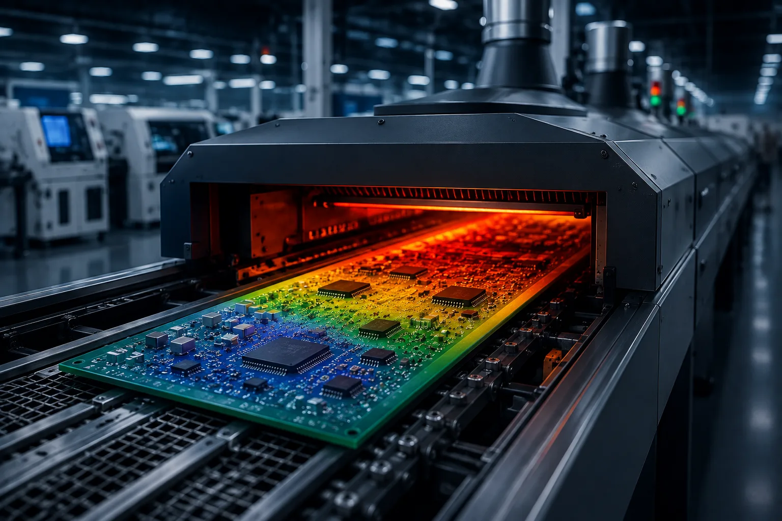
SMT PCB assembly moving through a multi-zone reflow soldering oven
For most modern SMT assemblies, solder paste printing and component placement are only part of the manufacturing process.
The PCB still needs to pass through a controlled thermal cycle that transforms the printed solder paste into permanent electrical and mechanical connections.
That process is reflow soldering.
At a high level:
→ Solder paste is deposited
→ Components are placed
→ PCB enters the reflow oven
→ Solder melts
→ Solder joints form
→ Assembly cools
The process sounds straightforward.
The engineering challenge is making it repeatable across the entire PCB.
A modern PCB can contain:
Each can respond differently to the same thermal cycle.
That is why reflow soldering is not simply about reaching a particular temperature.
It is about controlling time, temperature, heating rate, cooling rate and thermal uniformity throughout the assembly.
1. What Is Reflow Soldering?
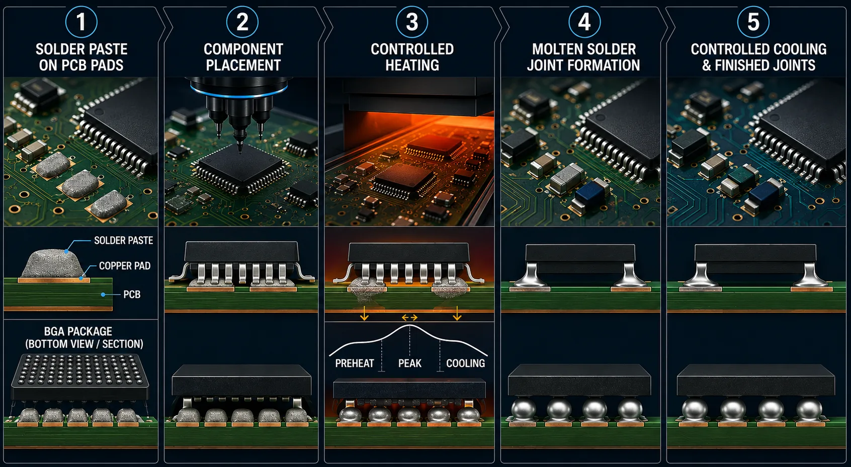
Reflow converts printed solder paste into permanent electrical and mechanical solder joints through a controlled thermal cycle.
Reflow soldering is an SMT process in which solder paste deposited on PCB pads is heated until the solder melts and forms solder joints between the PCB and components.
After the solder melts and wets the relevant surfaces, the assembly is cooled under controlled conditions.
The resulting solder joints provide:
Reflow is typically performed in a controlled multi-zone oven.
The thermal profile is developed around the requirements of the solder paste, PCB, components and assembly process.
2. Where Reflow Fits in SMT Assembly
Reflow does not operate as an isolated manufacturing step.
A typical SMT process looks like:
PCB preparation
↓
Solder-paste printing
↓
SPI
↓
Component placement
↓
Reflow soldering
↓
AOI
↓
X-ray where required
↓
Electrical testing
↓
Final inspection
The quality of reflow depends partly on what happens before it.
For example, reflow cannot compensate for severely incorrect solder-paste deposition.
Likewise, an excellent thermal profile cannot completely eliminate problems caused by poor PCB pad design.
This is why PCBA quality needs to be considered as a process chain, rather than as individual machines operating independently.
3. The Four Main Stages of a Reflow Profile
A typical reflow thermal profile can be broadly divided into:
The exact profile depends on the solder paste, component requirements, PCB construction and manufacturer's process window.
4. Stage 1 — Preheat
During preheat, the PCB assembly gradually increases in temperature.
The objective is to avoid excessive thermal shock while bringing the board toward the required process conditions.
A controlled heating rate is important.
If heating is too aggressive, it can contribute to:
The preheat stage therefore needs to be controlled rather than simply maximized for speed.
5. Stage 2 — Soak
The soak region allows the PCB assembly to approach a more uniform temperature.
Depending on the solder paste system, this stage can also support flux activation and help stabilize the assembly before the solder reaches melting temperature.
The purpose is not merely to "hold the board hot."
It is to help establish a controlled thermal condition before entering the reflow zone.
6. Stage 3 — Reflow
The assembly then reaches temperatures above the solder alloy's melting point.
The solder transitions from a solid/paste state to molten solder.
During this stage:
→ Solder melts
→ Surfaces become wetted
→ Solder joints form
→ Intermetallic interfaces develop
The assembly needs sufficient time above liquidus to achieve appropriate solder-joint formation without unnecessarily increasing thermal exposure.
7. Stage 4 — Cooling
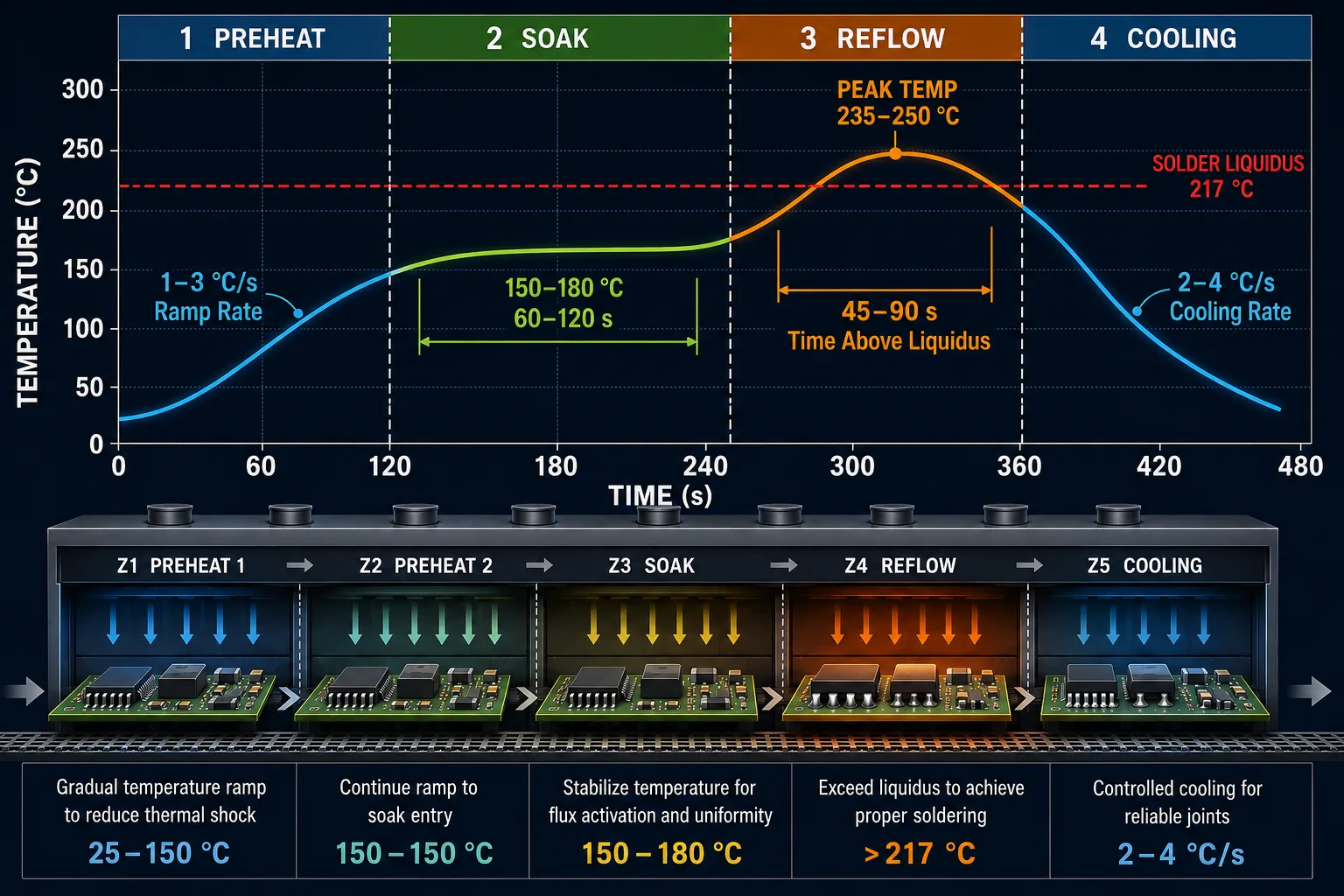
A reflow profile describes how PCB temperature changes throughout the soldering process.
After reflow, the assembly is cooled.
Cooling rate can influence the resulting solder microstructure and mechanical properties.
Extremely aggressive cooling can create thermal stress.
Insufficiently controlled cooling can affect throughput and process consistency.
The appropriate cooling conditions therefore need to be established as part of the overall thermal-profile development.
8. What Is a Thermal Profile?
A thermal profile is the measured temperature behavior of a PCB assembly as it moves through the reflow oven.
It is typically recorded using thermocouples attached to representative locations on the PCB.
The resulting graph helps engineers understand:
The profile can then be compared with the solder-paste manufacturer's recommended process window and relevant component requirements.
9. Why One Temperature Does Not Describe Reflow
A common misunderstanding is:
"The reflow oven is set to 240°C, so the PCB is reflowing at 240°C."
That is not how the process works.
The oven contains multiple heating zones.
The PCB temperature changes continuously as it travels through those zones.
More importantly, different areas of the PCB may reach different temperatures at different times.
For example:
A large copper plane may absorb heat differently from a small isolated pad.
A large BGA may behave differently from a small passive component.
A connector with substantial thermal mass may heat more slowly than nearby components.
Therefore, the PCB's measured thermal profile is more meaningful than simply looking at oven-zone setpoints.
10. Thermal Mass and PCB Design
PCB design has a direct impact on reflow behavior.
Factors include:
A large copper area can act as a thermal sink.
That can cause nearby areas to heat differently from less copper-dense portions of the board.
11. Large Components Can Create Thermal Challenges
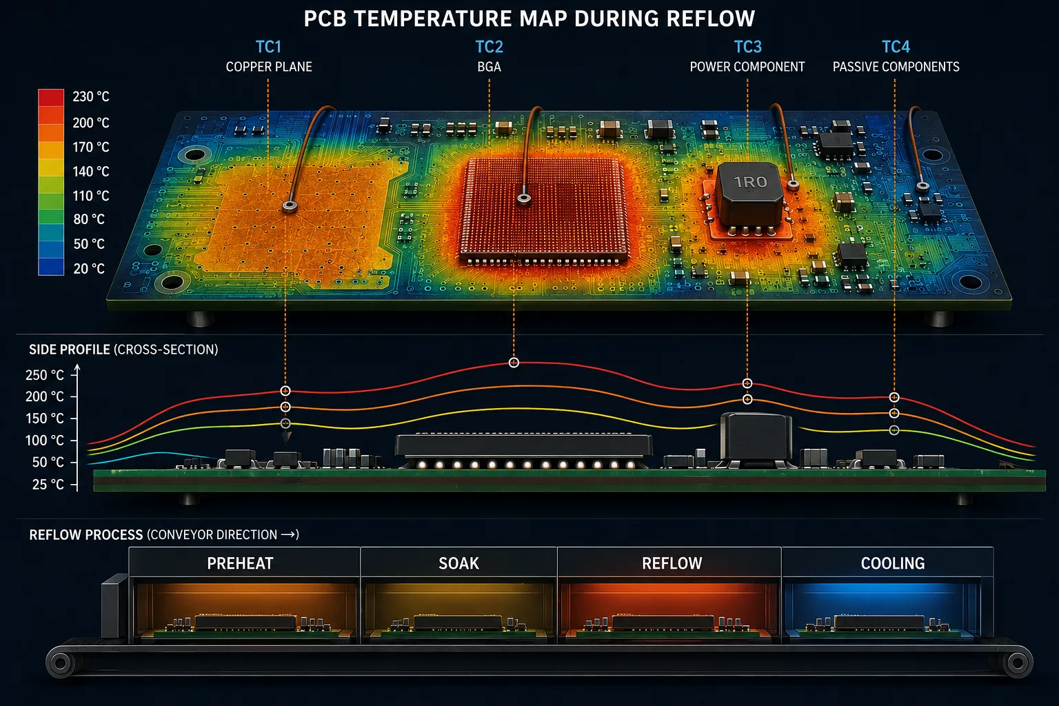
Copper distribution, component size and board construction can create thermal differences across a PCB during reflow.
Some components absorb considerably more heat than others.
Examples include:
If the profile is developed without considering these areas, the assembly may experience uneven soldering conditions.
This is why thermal profiling should use representative locations, including thermally challenging areas.
12. Lead-Free Reflow Soldering
Modern electronics manufacturing commonly uses lead-free solder alloys.
A widely used family of lead-free alloys is based on tin, silver and copper.
Lead-free processes generally require different thermal considerations from traditional tin-lead solder processes because the melting behavior and recommended process windows differ.
The correct profile should always be established against the specific solder paste/alloy manufacturer's recommendations.
13. Time Above Liquidus
One important parameter in reflow profiling is Time Above Liquidus (TAL).
This is the period during which the solder remains above its liquidus temperature.
The assembly needs enough time in this region for proper solder-joint formation.
However, more time is not automatically better.
Excessive thermal exposure can increase stress on components, materials and the PCB.
The goal is therefore a controlled process window rather than simply maximizing TAL.
14. Peak Temperature
Peak temperature is another important parameter.
The assembly must reach a sufficient temperature to properly melt and form the solder joints.
However, the peak should remain within the process limits appropriate for the solder alloy, components and PCB materials.
A profile that is too cold may cause poor soldering.
A profile that is too hot may increase thermal risk.
This is why thermal profiling needs to be based on actual measurements rather than assumptions.
15. Common Reflow Soldering Defects
Reflow-related defects can include:
Importantly, not every defect originates exclusively in the reflow oven.
Soldering defects often result from interactions among:
PCB design
Stencil design
Solder paste
Component condition
Placement
Thermal profile
16. Tombstoning
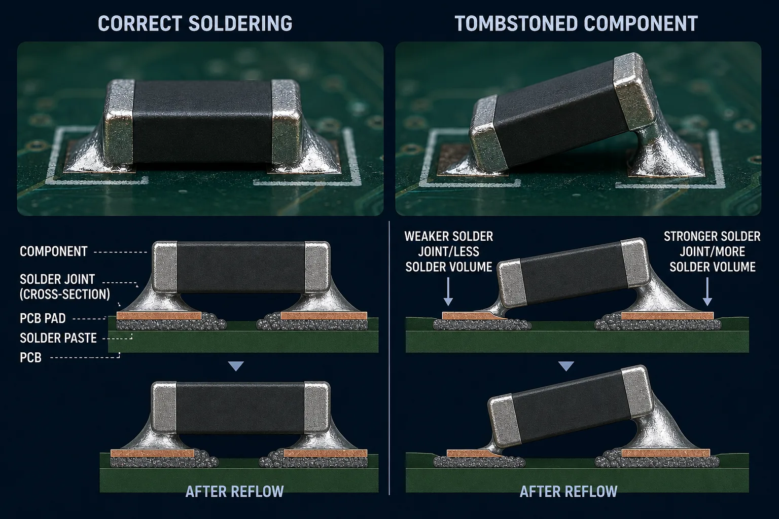
Tombstoning occurs when an SMT component becomes lifted or rotated during soldering due to unequal forces at its two terminals.
Tombstoning occurs when one end of a small two-terminal component lifts from the PCB during reflow.
It is commonly associated with unequal forces acting on the two ends of the component.
Potential contributors include:
Stencil design and PCB layout can therefore influence tombstoning risk.
17. Solder Bridging
Solder bridging occurs when molten solder creates an unintended connection between adjacent conductive features.
Potential contributing factors include:
This illustrates an important point:
Not every solder defect should be "fixed" by changing the reflow profile.
If the root cause is excessive solder-paste deposition, modifying the thermal profile may not solve the underlying problem.
18. Poor Wetting
Good soldering requires molten solder to properly wet the intended surfaces.
Poor wetting can be influenced by:
The correct root cause should therefore be established before changing process parameters.
19. Voiding
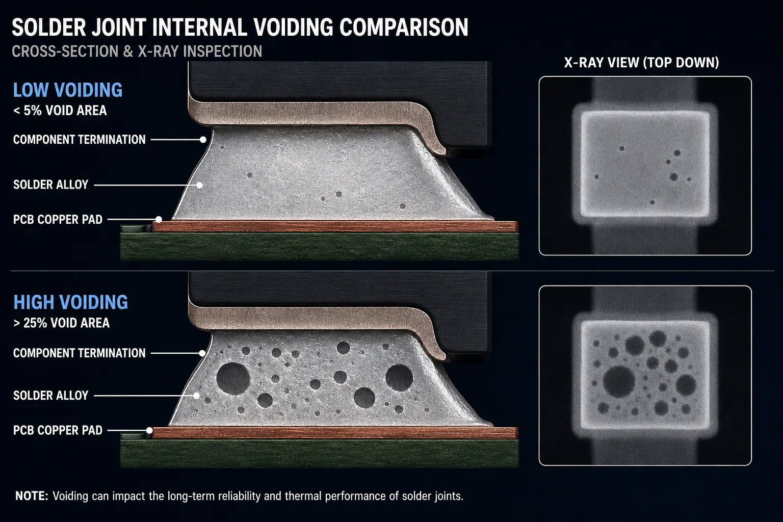
X-ray inspection can reveal internal solder-joint voiding that conventional visual inspection cannot see.
Voids are internal areas within a solder joint where gas or other material prevents complete solder continuity.
Voiding can occur in various SMT joints.
For certain components, particularly large thermal pads and power-related connections, voiding can be particularly important because it may influence thermal and mechanical performance.
X-ray inspection can be used to evaluate internal solder-joint characteristics that are not visible from the PCB surface.
20. Head-in-Pillow Defects in BGA
BGA assemblies introduce additional reflow challenges.
One example is head-in-pillow, where the BGA solder ball and solder paste do not form the intended metallurgical connection.
Potential contributors include:
Because the joint is hidden beneath the BGA package, X-ray inspection is often important when investigating BGA-related defects.
21. Component and PCB Warpage
Thermal expansion occurs during heating.
The PCB and components may respond differently because their materials have different thermal characteristics.
Large packages and large PCBs can therefore be particularly sensitive to warpage.
Excessive deformation can affect:
Warpage should therefore be considered during both design and process development.
22. Reflow and Moisture-Sensitive Components
Some electronic packages have moisture-sensitivity requirements.
If moisture is absorbed into a package and the component is subjected to a high-temperature reflow process, the resulting internal stresses can potentially damage the package.
Manufacturers therefore need to follow the relevant component handling and moisture-sensitivity requirements specified by the component manufacturer.
This may involve:
23. How Thermal Profiles Are Developed
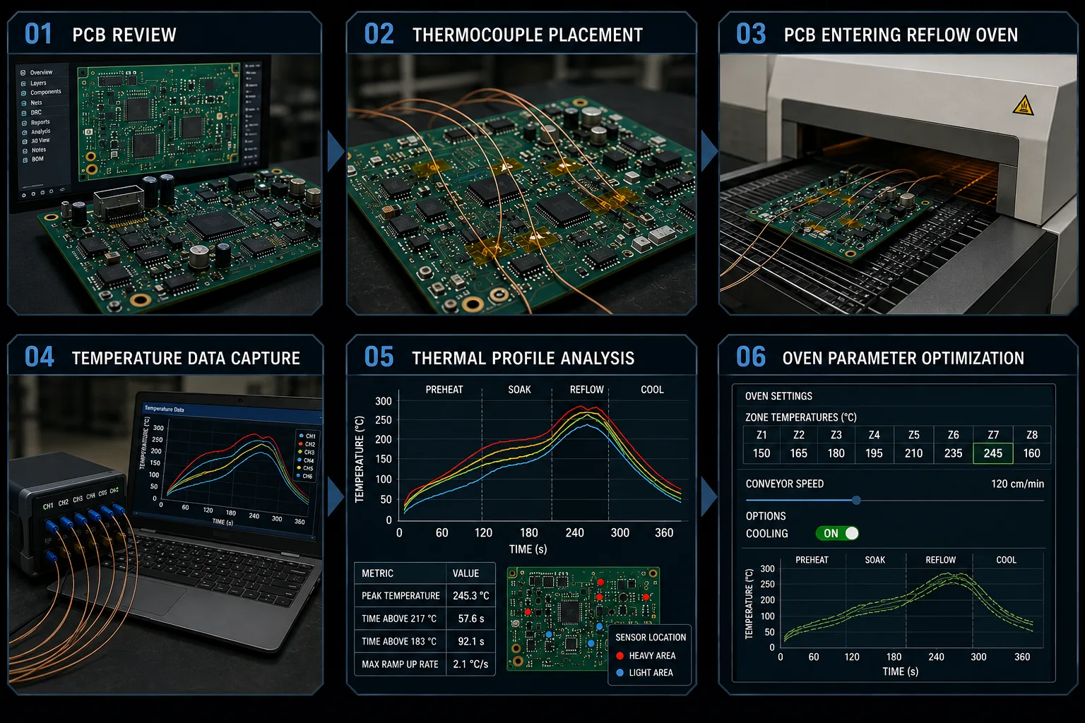
Thermal profiling uses measured PCB temperatures to establish a controlled and repeatable reflow process.
A practical profile-development process may involve:
Step 1 — Review the assembly
Identify:
Step 2 — Review solder paste requirements
Check the manufacturer's recommended:
Step 3 — Attach thermocouples
Place thermocouples at representative hot and cold locations.
Step 4 — Run the board through the oven
Record actual PCB temperatures.
Step 5 — Analyze the profile
Compare measurements against the required process window.
Step 6 — Adjust oven settings
Modify zone temperatures, conveyor speed or other relevant parameters.
Step 7 — Validate
Repeat the measurement until the required process window is achieved consistently.
24. Why Thermocouple Placement Matters
A thermal profile is only as useful as the measurements behind it.
Thermocouples should be placed at representative locations rather than randomly.
Typical considerations include:
The objective is to understand the thermal extremes and establish an appropriate process window.
25. Reflow Profile Verification
A profile developed for one PCB configuration should not automatically be assumed to work for every product.
Changes in:
can affect the thermal response.
Profile verification is therefore particularly important during:
26. Reflow for BGA Assemblies
BGA packages deserve particular attention because their solder joints are hidden beneath the component.
The process must achieve adequate solder-joint formation across the entire BGA footprint.
Factors include:
X-ray inspection can provide valuable visibility after reflow.
27. Reflow for QFN Assemblies
QFN packages can also be sensitive to solder-volume and thermal-pad conditions.
If excessive solder is deposited beneath the exposed thermal pad, the package can potentially float or tilt during reflow.
This is why:
Stencil aperture design
and
Reflow profile
must be considered together.
28. Reflow Defect Troubleshooting
When a defect appears, changing the thermal profile should not automatically be the first response.
A structured investigation can ask:
1. Is the solder-paste deposit correct?
Check SPI data.
2. Is the component positioned correctly?
Check placement data and AOI.
3. Is the PCB pad/footprint correct?
Review the design.
4. Is the surface finish appropriate?
Review PCB fabrication data.
5. Is the solder paste within specification?
Check storage, age and process condition.
6. Is the thermal profile within the required window?
Review actual thermal measurements.
7. Is there a package or PCB warpage issue?
Investigate if relevant.
This approach is more reliable than adjusting oven settings based only on the visible symptom.
29. Common Defects and Potential Root Causes
| Defect | Potential contributing factors |
|---|---|
| Tombstoning | Paste imbalance, pad design, thermal imbalance, placement |
| Bridging | Excess paste, aperture design, fine pitch, alignment |
| Poor wetting | Oxidation, contamination, paste or profile |
| Voiding | Paste chemistry, pad design, thermal conditions |
| Head-in-pillow | Warpage, oxidation, paste/profile conditions |
| Opens | Insufficient paste, poor wetting, placement, warpage |
| Solder balls | Paste/process conditions, printing or reflow |
| Component displacement | Placement, solder volume, reflow forces |
| Excessive intermetallic growth | Excessive thermal exposure |
| Pad/component damage | Excessive thermal stress or unsuitable profile |
These are potential contributing factors, not universal diagnoses. Actual root-cause analysis should be based on process data and inspection evidence.
30. Reflow and PCB Design
PCB designers can influence reflow performance through:
For example, highly asymmetric copper distribution around a small passive component can contribute to unequal heating and soldering forces.
Good DFM review should therefore consider thermal behavior, not only whether the PCB can physically be fabricated.
31. Reflow and Stencil Design Are Closely Connected
A useful way to think about the relationship is:
Stencil determines solder-paste volume
↓
Placement determines component position
↓
Reflow determines how that solder forms the joint
If solder-paste volume is incorrect, the reflow profile cannot necessarily compensate.
Likewise, a good stencil does not eliminate the need for an appropriate thermal profile.
Reliable SMT manufacturing requires all three stages to work together.
32. What Should You Ask a PCBA Supplier About Reflow?
When evaluating a manufacturing partner, ask:
Thermal Process
Profiling
Process Control
Inspection
NPI
These questions can distinguish a supplier with genuine process engineering capability from one that simply operates an SMT line.
33. Reflow Process Control Checklist
Before production, verify:
Solder Paste
PCB
Stencil
Reflow
Inspection
34. Reflow During NPI
NPI is where reflow process development becomes particularly valuable.
The objective is not simply to make the first board work.
It is to establish a process that can be repeated.
During NPI, the manufacturing team can evaluate:
→ PCB
→ Stencil
→ Paste
→ Placement
→ Reflow
→ Inspection
→ Yield
The results can then be used to establish the production process.
This is especially important when the board contains:
35. From Prototype to Production
A prototype may be assembled successfully under controlled conditions.
But production introduces additional requirements:
The reflow process therefore needs to move from:
"We achieved a good board."
to:
"We have a controlled process capable of repeatedly producing good boards."
That distinction becomes increasingly important as production volume grows.
36. Final Takeaway
Reflow soldering is the thermal process that converts solder paste into functional SMT solder joints.
But reliable reflow is not simply about heating a PCB until solder melts.
It requires control of:
Temperature
Time
Heating rate
Time above liquidus
Cooling
Thermal uniformity
PCB/component behavior
The most reliable approach is to develop and validate a product-specific thermal profile based on actual PCB measurements and the requirements of the solder paste and components.
And when defects occur, the correct question is not simply:
"What should we change in the reflow oven?"
It is:
"Where in the assembly process did the defect originate, and what evidence supports the root cause?"
That mindset is fundamental to reliable PCBA manufacturing.
37. QUADRIONIX PERSPECTIVE
At QUADRIONIX, reflow is treated as one element of a connected manufacturing process rather than an isolated production step.
For complex assemblies, the critical chain is:
→ PCB Design
→ Stencil Design
→ Solder-Paste Deposition
→ Component Placement
→ Thermal Profiling
→ Reflow
→ AOI / X-Ray
→ Electrical Testing
→ Production Process Control
For BGA, QFN, fine-pitch and thermally challenging assemblies, this integrated approach becomes particularly important.
A good manufacturing partner should be able to explain how the thermal profile is developed, measured, validated and controlled—not merely state that the PCB passes through a reflow oven.
If you Need a Controlled SMT Reflow Process for Your PCBA, Quadrionix team can review your assembly requirements from a DFM, stencil, thermal-process, inspection and production-readiness perspective.
From precision SMT assembly to production-ready PCBA — engineered for reliability and repeatability.
Frequently Asked Questions
Ready to manufacture your electronics project?
Upload your Gerber files & BOM for automated DFM review, engineering feedback, and guaranteed delivery timelines.