PCB Testing Methods Explained: AOI, X-Ray, ICT, Flying Probe and Functional Testing
How AOI, X-Ray, ICT, Flying Probe and Functional Testing work, what defects they catch, and how to build an effective testing strategy for PCB fabrication and assembly.
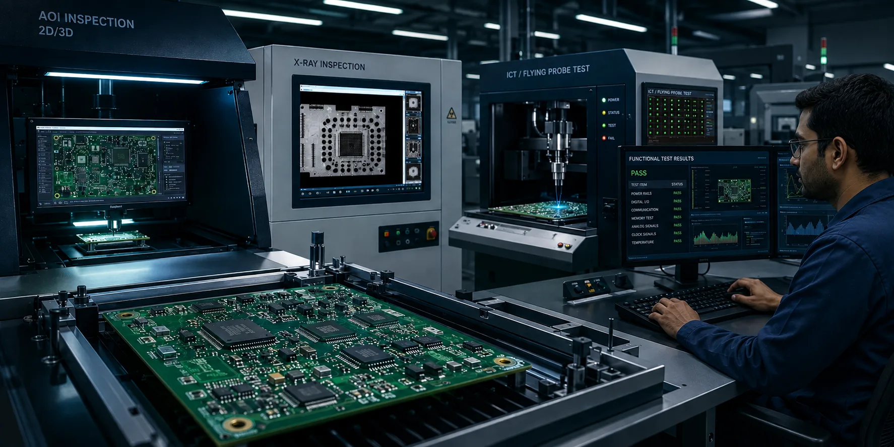
PCB assembly testing using AOI X-ray ICT flying probe and functional testing
A PCB assembly can look perfect and still contain a hidden defect.
A solder joint may be incomplete.
A BGA connection may be defective beneath the package.
A component may be incorrectly placed.
A resistor may have the wrong value.
A short circuit may exist between two nets.
Or every physical connection may appear correct while the finished assembly still fails to perform its intended function.
This is why PCB inspection and testing are not the same thing.
Modern PCBA manufacturing uses multiple testing and inspection techniques, each designed to answer different questions.
Some methods primarily examine:
"Was the PCB assembled correctly?"
Others ask:
"Are the electrical connections correct?"
And functional testing asks the most important system-level question:
"Does the finished assembly actually work as intended?"
The five methods most commonly encountered in professional PCB/PCBA manufacturing are:
The right approach is rarely about choosing one method.
It is about building a test strategy appropriate to the product, technology, risk, volume and production stage.
1. Why PCB Testing Matters
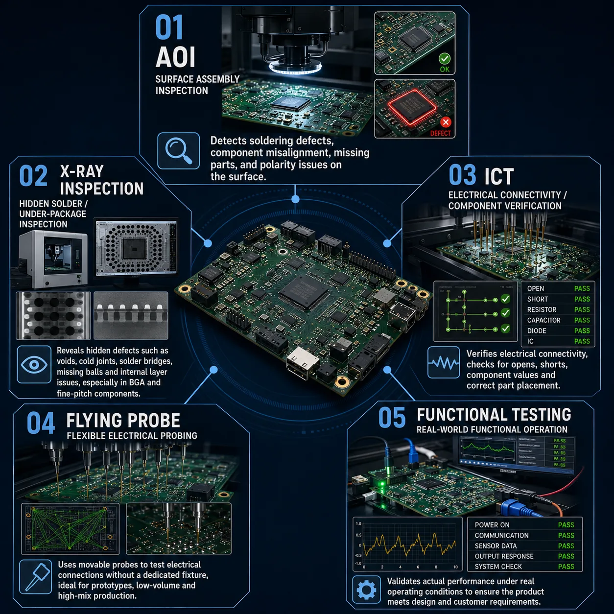
Different PCB testing methods detect different classes of manufacturing and functional defects.
PCB assembly contains many opportunities for manufacturing variation.
Examples include:
Some can be detected visually.
Some require electrical testing.
Others can only be identified by operating the assembled product.
This creates an important principle:
No single PCB test method detects every type of defect.
2. Inspection vs Testing: What Is the Difference?
Before comparing methods, it helps to distinguish inspection from testing.
Inspection
Inspection primarily evaluates whether the physical assembly appears correct.
Examples:
Electrical testing
Electrical testing evaluates electrical characteristics or connectivity.
Examples:
Functional testing
Functional testing evaluates whether the assembled PCB performs its intended operation.
This distinction is important because a PCB can pass one category and fail another.
For example:
A PCB may pass AOI because every component appears correctly positioned.
But it could still fail functional testing because of an electrical or component-level problem that optical inspection cannot identify.
3. AOI — Automated Optical Inspection
AOI uses cameras and software to inspect PCB assemblies automatically.
The system captures images of the PCB and compares the observed assembly against defined criteria or reference information.
AOI can identify issues such as:
AOI is particularly valuable in SMT manufacturing because large numbers of components can be inspected quickly and consistently.
4. What AOI Does Well
AOI is particularly effective for visible surface-level defects.
For example:
Component placement
Is the component positioned where it should be?
Component presence
Is a component missing?
Orientation
Is the component rotated or reversed?
Solder appearance
Does the visible solder joint appear acceptable?
Pattern comparison
Does the assembly correspond to the expected design?
AOI provides an important automated inspection layer without requiring manual visual inspection of every component.
5. AOI Limitations
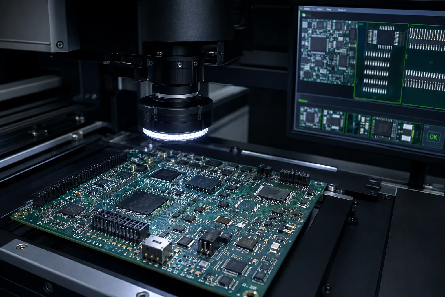
AOI provides automated visual inspection of visible PCB assembly features.
AOI cannot see everything.
A camera generally cannot directly inspect connections hidden underneath components.
This is particularly relevant for:
AOI may also identify an apparent anomaly that requires engineering review.
Therefore:
AOI is powerful, but it is not a complete substitute for electrical or X-ray testing.
6. When Should AOI Be Used?
AOI is particularly useful for:
It can also be useful at multiple stages of the assembly process depending on the manufacturer's process architecture.
The key advantage is speed and repeatability.
7. X-Ray Inspection
X-Ray inspection provides visibility into structures that cannot be adequately inspected from the PCB surface.
This makes it particularly valuable for assemblies containing:
X-ray systems use X-rays to generate an image based on differences in material density.
This can reveal defects that optical inspection cannot see.
8. What Can X-Ray Inspection Detect?
Depending on the equipment and application, X-ray inspection can help identify:
For example, a BGA may contain hundreds of solder connections beneath the package.
AOI cannot directly see those connections.
X-ray inspection can provide visibility into them.
9. Why BGA Makes X-Ray Important
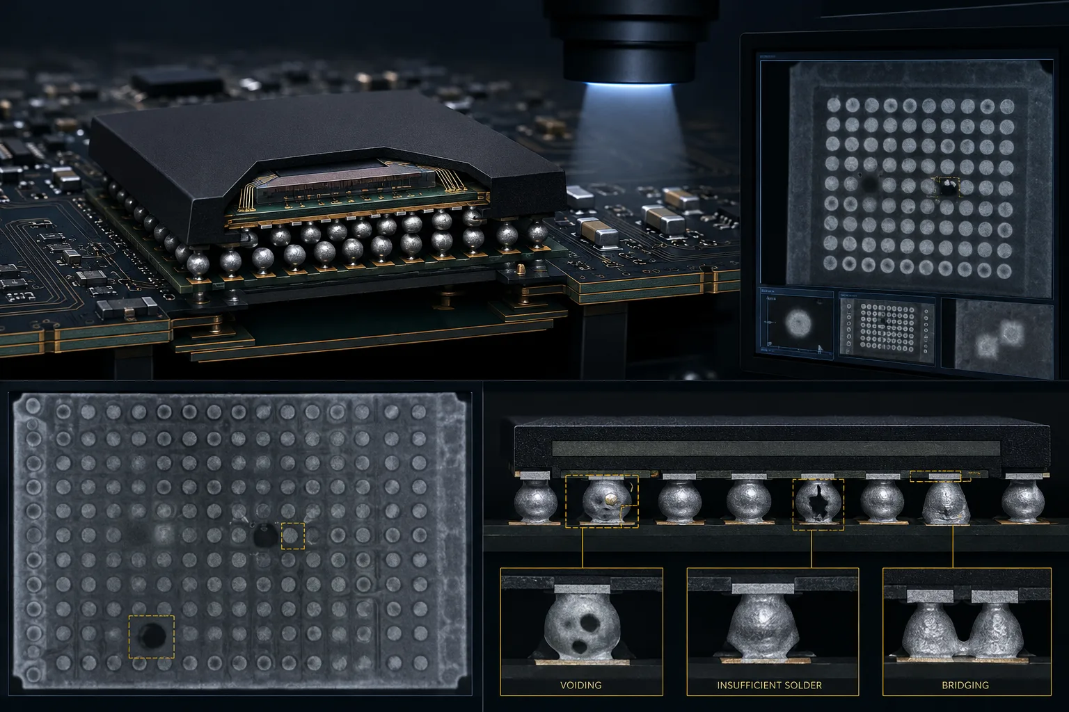
X-ray inspection provides visibility into solder connections hidden beneath packages such as BGAs.
BGA packages illustrate the limitations of surface inspection.
The solder connections exist beneath the component.
Therefore:
Visible inspection → limited
X-ray inspection → internal visibility
This does not mean every BGA assembly automatically requires the same level of X-ray inspection.
The appropriate approach depends on:
10. X-Ray Limitations
X-ray inspection is not a universal solution.
Depending on the system and application, it may involve:
Therefore, X-ray should generally be deployed where its additional visibility provides meaningful quality value.
11. ICT — In-Circuit Test
In-Circuit Test evaluates the electrical characteristics and connectivity of a PCB assembly using dedicated test points and a test fixture.
ICT can potentially verify:
ICT is different from AOI because it is not primarily looking at the physical appearance of the assembly.
It is electrically evaluating the board.
12. How ICT Works
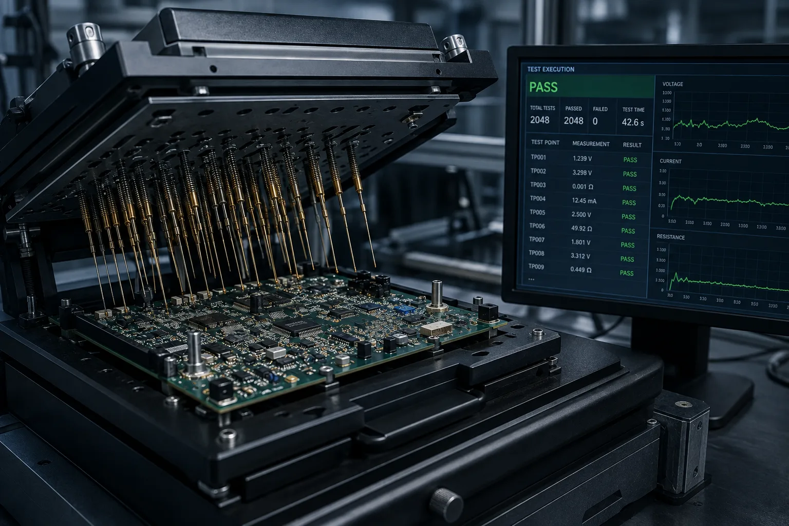
ICT uses a dedicated fixture and test points to perform electrical checks on the PCB assembly.
A typical ICT setup involves:
PCB assembly
↓
Test fixture
↓
Contact with defined test points
↓
Electrical measurements
↓
Pass / Fail results
The fixture is designed around the PCB and its test-point architecture.
This makes test-point planning an important part of PCB design for products expected to use ICT.
13. Advantages of ICT
ICT can provide:
It can be particularly attractive for:
14. ICT Limitations
ICT typically requires a dedicated fixture.
That creates:
Therefore, ICT economics often become more attractive as production volume increases.
A rapidly changing prototype may not justify a dedicated ICT fixture.
15. Flying Probe Testing
Flying probe testing provides electrical testing without requiring a traditional dedicated ICT fixture.
Instead, multiple programmable probes move across the PCB to contact selected test points.
This provides greater flexibility.
Flying probe is particularly useful for:
16. Flying Probe vs ICT
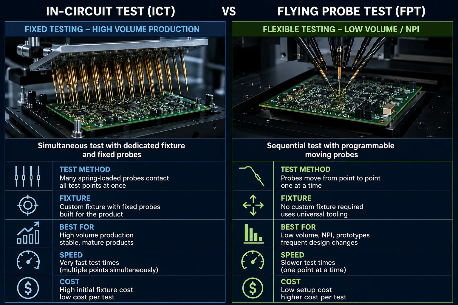
ICT and flying probe both provide electrical testing, but their economics and flexibility differ.
The basic difference is:
ICT
Dedicated fixture + high-speed repetitive testing
Flying Probe
Programmable probes + greater flexibility
A simplified comparison:
| Factor | ICT | Flying Probe |
|---|---|---|
| Dedicated fixture | Usually required | Usually not |
| Initial cost | Higher | Lower |
| Flexibility | Lower | Higher |
| PCB changes | More costly | Easier |
| High volume | Strong fit | Less ideal |
| Prototype/NPI | Less attractive | Strong fit |
| Test speed | Generally faster | Generally slower |
The actual suitability depends on the specific product and test requirements.
17. Functional Testing
Functional testing asks a different question:
Does the assembled PCB perform its intended function?
Instead of simply checking individual connections, functional testing attempts to operate the product—or a representative portion of it—under defined conditions.
Depending on the product, this could include:
Functional testing is therefore closely tied to the product's actual design requirements.
18. Functional Testing vs ICT
This distinction is extremely important.
ICT
Primarily asks:
"Are the electrical components and connections behaving as expected at the test points?"
Functional Test
Primarily asks:
"Does the assembled product perform its intended function?"
A board could pass many electrical checks and still fail a functional requirement.
For example:
A communications board may pass continuity and component checks but fail to establish the required communication link.
Functional testing can identify that system-level problem.
19. Functional Testing Is Product-Specific
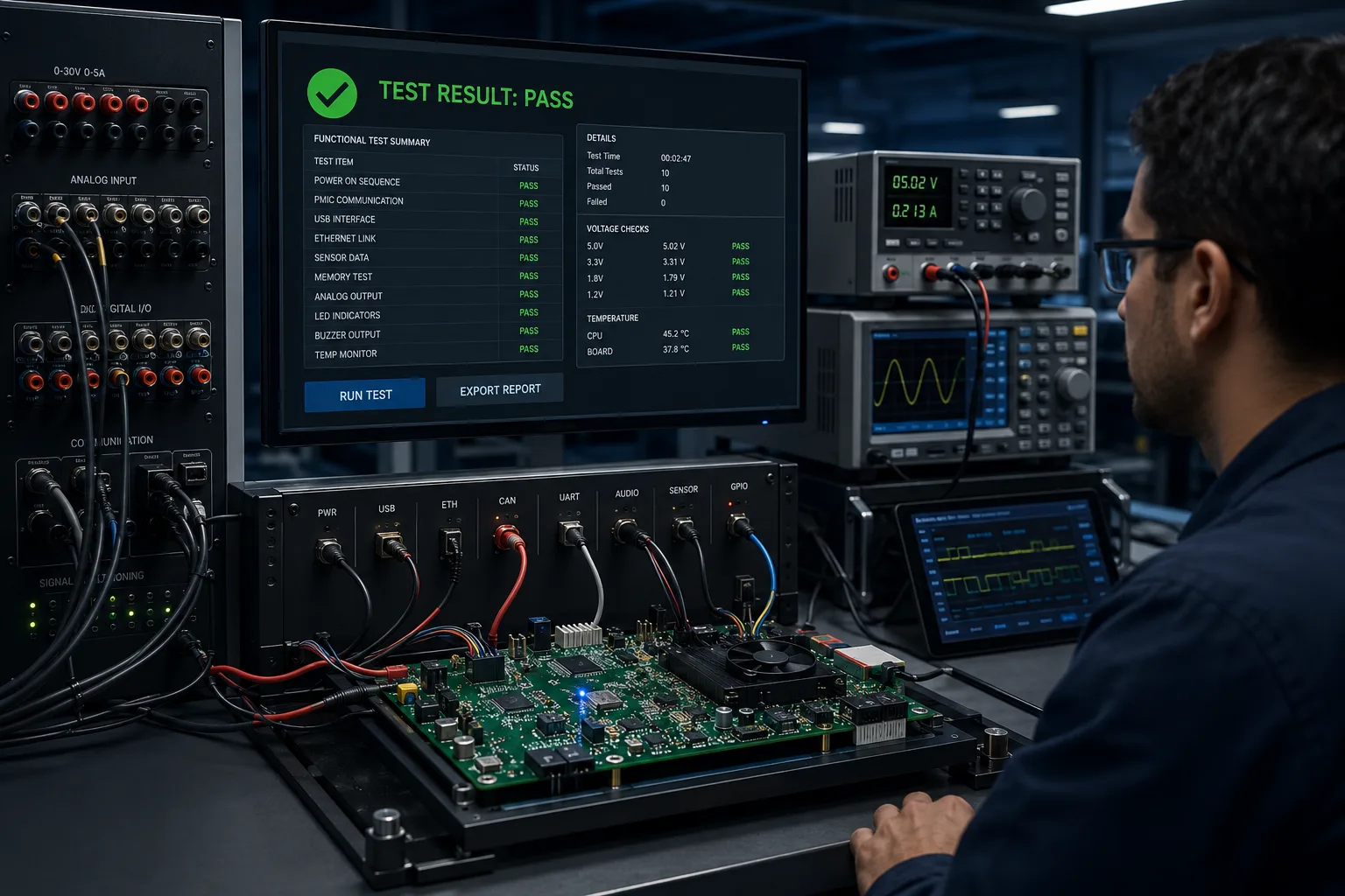
Functional testing validates whether the assembled PCB performs its intended product-level operation.
Unlike AOI, which can inspect many types of PCBs using generalized inspection principles, functional testing is closely tied to the product.
A medical electronics assembly, industrial controller and consumer device will have very different functional requirements.
A functional test system may therefore include:
This makes functional testing an engineering activity as much as a manufacturing activity.
20. Comparing the Five Main PCB Testing Methods
| Method | Primary Purpose | Hidden Defects | Electrical Testing | Functional Testing | Typical Strength |
|---|---|---|---|---|---|
| AOI | Visual assembly inspection | Limited | No | No | Fast surface inspection |
| X-Ray | Internal inspection | Yes | No | No | BGA/hidden solder inspection |
| ICT | Electrical verification | No | Yes | Limited | High-volume electrical testing |
| Flying Probe | Electrical verification | No | Yes | Limited | Flexible NPI/low-volume testing |
| Functional Test | Product operation | Indirectly | Yes, depending on test | Yes | Real-world behavior |
The important point is not that one method is "best."
Each answers a different question.
21. AOI vs X-Ray: When Do You Need Both?
A common misconception is:
"If we have AOI, why do we need X-ray?"
The answer is visibility.
AOI examines what the camera can see.
X-ray examines internal structures that may not be visible optically.
For a simple SMT assembly with accessible solder joints, AOI may provide substantial inspection coverage.
For an assembly containing complex BGAs or hidden solder joints, X-ray may provide additional information.
The two methods can therefore be complementary.
22. ICT vs Flying Probe: Which Should You Choose?
The choice depends heavily on production conditions.
Choose ICT when:
Consider flying probe when:
The right answer depends on the actual manufacturing program.
23. What About Manual Visual Inspection?
Manual inspection still has a place.
An experienced technician can identify:
But manual inspection has limitations in:
For production environments, automated inspection and testing can provide stronger process control when properly implemented.
24. Testing Should Start at PCB Design
Testing is not something that should be added at the end of manufacturing.
Design teams should consider:
This is part of Design for Testability (DFT).
A PCB that is easy to manufacture but difficult to test can create avoidable production challenges.
25. Test Coverage Matters More Than Test Equipment Count
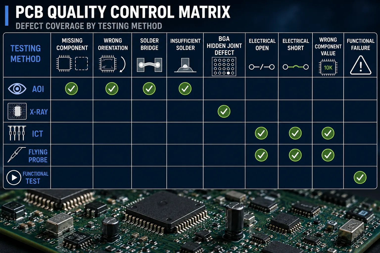
Test coverage depends on matching each inspection or test method to the defects it can realistically detect.
A factory having many types of testing equipment does not automatically mean the product has excellent test coverage.
The more important question is:
Which defects can the selected test strategy actually detect?
For example:
AOI
may detect visible placement defects.
X-Ray
may detect hidden solder defects.
ICT
may detect certain electrical faults.
Functional testing
may detect product-level failures.
The strongest strategy connects these capabilities around the actual defect risks.
26. Prototype Testing vs Production Testing
Testing strategy should evolve with the product.
Prototype
Focus:
NPI
Focus:
Pilot Production
Focus:
Volume Production
Focus:
27. Testing and Production Yield
Testing should not simply be viewed as a way to reject defective boards.
Test data can reveal patterns.
For example:
If AOI identifies repeated solder defects in the same area, the manufacturing process may require adjustment.
If ICT repeatedly identifies a particular electrical issue, the assembly process or component may need investigation.
If functional testing identifies intermittent failures, engineering may need to investigate both design and manufacturing factors.
This creates a feedback loop:
Test → Data → Root Cause → Process Improvement → Better Yield
28. Test Data and Traceability
For professional production programs, test results can become valuable manufacturing records.
Depending on customer and product requirements, traceability may include:
This can become particularly important for regulated or mission-critical products.
29. How to Choose the Right PCB Testing Strategy
A practical decision framework begins with:
Step 1 — Understand the product
What does the PCB do?
Step 2 — Identify likely defects
What can fail during assembly?
Step 3 — Identify component technologies
Are there:
Step 4 — Understand production volume
Prototype?
Low volume?
Medium volume?
High volume?
Step 5 — Evaluate PCB testability
Are suitable test points available?
Step 6 — Define functional requirements
What must the finished assembly actually do?
Step 7 — Build the test coverage
Select the appropriate combination of:
AOI + X-Ray + ICT/Flying Probe + Functional Test
rather than choosing equipment in isolation.
30. A Practical PCB Testing Decision Matrix
| Situation | Potentially Useful Testing |
|---|---|
| Standard SMT production | AOI |
| Fine-pitch SMT | AOI + electrical testing |
| BGA-heavy assembly | AOI + X-Ray |
| Prototype | Flying probe + functional testing |
| NPI | AOI + flying probe + functional testing |
| Stable high-volume product | AOI + ICT + functional testing |
| High-risk/complex assembly | AOI + X-Ray + electrical + functional |
| Product-specific performance requirements | Functional testing |
This is a planning framework—not a universal prescription.
The appropriate test strategy should be defined based on actual product and process requirements.
31. Questions to Ask a PCBA Manufacturing Supplier
Before selecting a manufacturing partner, ask:
Inspection
X-Ray
Electrical testing
Functional testing
Quality data
NPI
These questions help distinguish a supplier that simply assembles boards from one that can support a more complete manufacturing-quality process.
32. PCB Testing Checklist
Before moving into production, review:
Inspection
Electrical testing
Functional testing
Production
33. The Goal Is Not "More Testing"
More testing does not automatically mean better manufacturing.
The goal is:
The right testing for the right risks at the right production stage.
An unnecessarily complex test strategy can increase:
An inadequate strategy can increase:
The objective is balance.
34. A Strong PCB Quality Strategy Is Layered
A robust manufacturing process may look like:
Incoming component control
↓
SMT process control
↓
AOI
↓
X-Ray where appropriate
↓
ICT / Flying Probe
↓
Functional Testing
↓
Final inspection
↓
Traceability & release
Not every product requires every layer.
But the concept is important:
Different controls catch different failure modes.
35. FINAL TAKEAWAY
PCB testing is not a single activity.
It is a combination of inspection and validation methods designed to identify different classes of manufacturing and functional defects.
AOI
Best suited to automated visual inspection of visible assembly features.
X-Ray
Provides visibility into hidden structures such as BGA solder connections.
ICT
Provides fast, repeatable electrical testing for suitable production environments.
Flying Probe
Provides flexible electrical testing particularly useful for prototypes, NPI and lower-volume production.
Functional Testing
Validates whether the assembled PCB actually performs its intended function.
The strongest manufacturing strategy is therefore not:
"Which test is best?"
It is:
"Which combination of inspection and testing provides appropriate coverage for this product, process and production volume?"
That question should be answered during design and NPI, not after production problems appear.
36. QUADRIONIX PERSPECTIVE
At QUADRIONIX, PCB assembly quality is viewed as more than visual workmanship.
A production-ready PCBA process should connect:
Design for Testability
→ Manufacturing Process Control
→ Inspection
→ Electrical Verification
→ Functional Validation
→ Traceability
The appropriate combination depends on the PCB's technology, complexity, production volume and product requirements.
For international customers, this approach helps create a manufacturing process in which quality is designed into the production flow rather than treated as a final inspection step.
QUADRIONIX's objective is to help customers move from:
"The PCB was assembled."
to:
"The PCB was manufactured, inspected, tested and validated against defined requirements."
Before approving a manufacturing partner, determine:
Frequently Asked Questions
Ready to manufacture your electronics project?
Upload your Gerber files & BOM for automated DFM review, engineering feedback, and guaranteed delivery timelines.