PCB Material Selection: FR-4, High-Tg, High-Speed and Specialty Materials
A Practical Guide to Choosing PCB Laminates Based on Thermal Performance, Signal Integrity, Reliability, Cost and Manufacturing Requirements
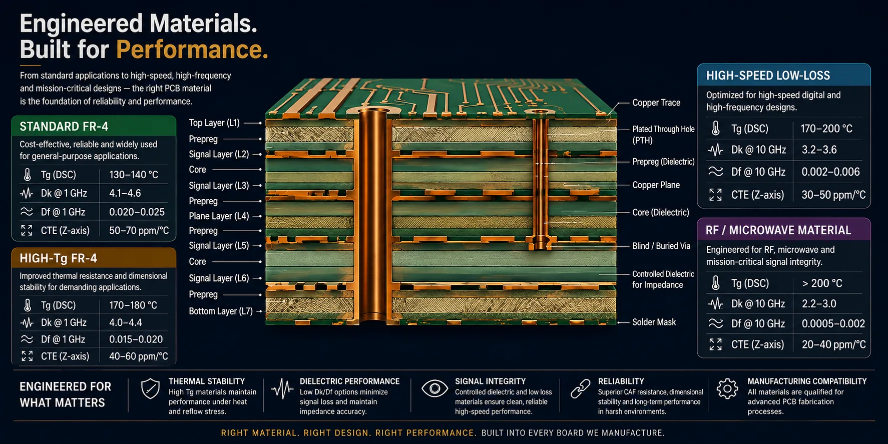
PCB laminate material selection showing FR-4 high-Tg high-speed and specialty materials
Choosing a PCB material is often treated as a procurement decision:
"Which laminate is available and how much does it cost?"
For straightforward electronics, that approach may be sufficient.
For demanding products, it is not.
The PCB laminate is part of the electrical, thermal, mechanical and manufacturing architecture of the product.
Material selection can influence:
This is why the correct question is not:
"Is FR-4 good enough?"
It is:
"What material properties does this PCB actually require, and can those properties be achieved reliably and economically with the intended manufacturing process?"
For many electronic products, standard FR-4 remains an excellent and highly practical starting point.
But as thermal, mechanical or electrical requirements become more demanding, the material specification may need to change.
1. What Is PCB Laminate?
A PCB is not simply copper laminated onto plastic.
A typical multilayer PCB contains combinations of:
The dielectric material separates conductive layers and contributes to both the mechanical and electrical behavior of the board.
For multilayer designs, the final PCB stack-up is determined by the combination of core and prepreg constructions.
IPC-4101 defines requirements for base materials, including laminate and prepreg used primarily for rigid and multilayer printed boards.
This means "PCB material" should be understood as more than simply a material name such as FR-4.
The actual construction can involve a specific material family, resin system, glass style, resin content, thickness and copper configuration.
2. Why FR-4 Is So Widely Used
FR-4 is the workhorse material family for a huge range of rigid PCBs.
Its popularity comes from a combination of:
That makes FR-4 an excellent choice for many:
But "FR-4" is not one single material formulation with identical properties from every supplier.
Different FR-4 systems can have significantly different:
Therefore:
Specifying only "FR-4" may be insufficient for a demanding production design.
3. What Does FR-4 Actually Mean?
FR-4 is broadly associated with flame-retardant glass-reinforced epoxy PCB materials.
However, the material family includes different formulations and performance grades.
IPC material specifications distinguish different material constructions and performance characteristics rather than treating all laminate as identical.
For example, IPC documentation includes FR-4 specifications covering different Tg ranges, including approximately 110–150°C and 150–200°C categories depending on the specification.
So when someone says:
"Use FR-4."
the next engineering questions should be:
That is where proper material selection begins.
4. The Most Important PCB Material Properties
When comparing PCB materials, engineers commonly evaluate several properties.
The most important ones include:
Thermal
Electrical
Mechanical
Environmental
Manufacturing
Economic
No single property determines whether a material is "better."
The correct material depends on the application.
5. Tg: What Is Glass Transition Temperature?
Tg, or glass transition temperature, is one of the most frequently discussed PCB laminate properties.
It describes the temperature region at which the resin system transitions from a relatively rigid glassy state toward a more rubber-like state.
For PCB design, Tg is important because material behavior changes significantly around this transition.
A higher Tg material can provide greater thermal margin for applications involving:
But there is an important misconception:
Higher Tg does not automatically mean a PCB is better for every application.
A material with a higher Tg may still be the wrong choice if its electrical properties, fabrication compatibility or cost do not fit the design.
6. High-Tg FR-4: When Does It Make Sense?
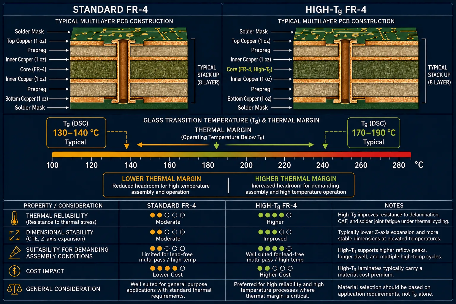
High-Tg FR-4 can provide greater thermal margin, but material selection should be based on the complete application rather than Tg alone.
High-Tg FR-4 is generally considered when the design needs greater thermal performance or reliability margin than a conventional lower-Tg material provides.
Potential applications include:
The important point is that high-Tg is a design requirement, not simply a premium upgrade.
If the application does not benefit from the additional thermal capability, paying for it may provide little practical value.
7. Tg Is Not the Same as Maximum Operating Temperature
This distinction is critical.
Tg should not be interpreted as:
"The maximum temperature at which my PCB can operate."
A product's allowable operating temperature depends on the complete material system and product architecture.
Other parameters matter, including:
Therefore, material selection should consider the complete thermal profile rather than comparing Tg numbers alone.
8. Td: Decomposition Temperature
Td, or decomposition temperature, relates to the temperature at which significant thermal decomposition of the material occurs.
This is different from Tg.
A material can have a high Tg but still require evaluation of its decomposition behavior under extreme thermal exposure.
Td becomes particularly relevant when considering:
Therefore, a material comparison should not stop at Tg.
9. CTE: Coefficient of Thermal Expansion
CTE describes how much a material expands or contracts with temperature.
For PCB reliability, CTE is particularly important in the Z-axis.
Why?
Because plated through-holes contain copper extending through the PCB thickness.
During thermal cycling:
PCB dielectric expands → contracts → plated copper experiences mechanical stress
Repeated cycling can contribute to reliability problems if the material system and construction are not appropriate.
This becomes particularly important for:
10. Why Z-Axis CTE Matters
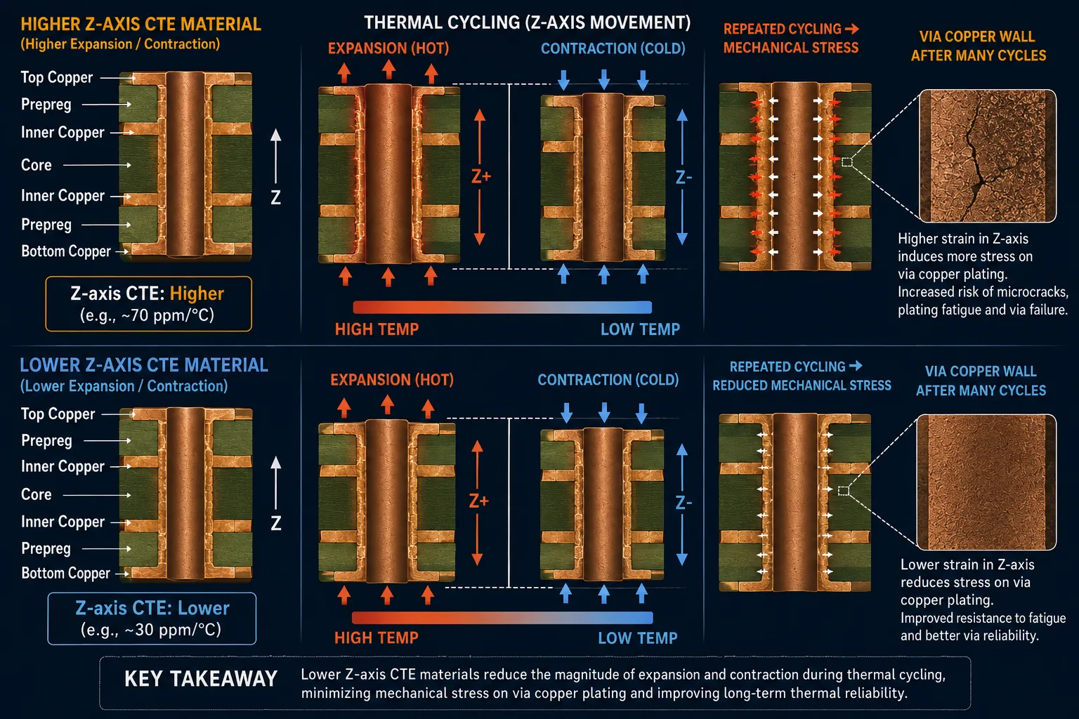
Z-axis thermal expansion is an important consideration for plated-through-hole reliability, particularly in demanding multilayer PCB applications.
Consider a multilayer board with many copper layers and plated through-holes.
The PCB expands differently in different directions.
The X-Y dimensional behavior affects:
The Z-axis behavior affects:
Some high-performance laminate systems are specifically engineered with lower z-axis CTE to improve plated-through-hole reliability. For example, published material data from high-performance laminate suppliers highlights z-axis CTE as an important reliability property.
11. Dk: Dielectric Constant
For high-speed and RF designs, dielectric constant, commonly represented as Dk, becomes increasingly important.
Dk influences electromagnetic propagation through the PCB dielectric.
It therefore affects:
A designer working on a controlled-impedance PCB cannot simply select a trace width independently of the laminate.
The relationship involves:
Trace geometry + dielectric thickness + Dk + reference plane
This is why material selection becomes part of signal-integrity engineering.
12. Df: Dissipation Factor
Df, also called loss tangent, indicates dielectric losses within the material.
For high-frequency signals, dielectric loss contributes to signal attenuation.
In general:
Lower Df → lower dielectric loss
although total signal loss also depends on conductor losses, roughness, geometry, frequency and other factors.
High-speed and RF materials therefore often emphasize low Df.
Published high-frequency laminate data illustrates how low-loss materials can achieve substantially lower Df values than conventional FR-4 systems.
13. Dk and Df Must Be Considered Together
It is tempting to compare two materials like this:
Material A: Dk 4.0
Material B: Dk 3.5
and conclude that B is automatically better.
That is not enough.
You should also consider:
For high-speed designs, consistency and predictability can be just as important as the absolute number.
14. Dk Is Not Always a Single Number
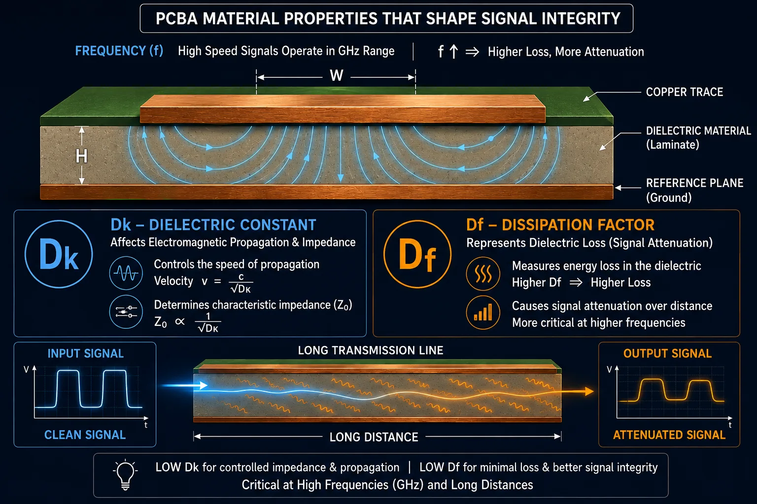
Dk influences transmission-line behavior and impedance, while Df is associated with dielectric loss and signal attenuation.
This is one of the more subtle areas of PCB material selection.
A material's effective dielectric behavior can vary depending on:
Material suppliers may therefore publish different Dk values for different purposes, including process and design values.
For example, Rogers publishes separate typical/process and design Dk information for several high-frequency materials.
This distinction matters when calculating controlled impedance.
15. What PCB Material Is Best for High-Speed Signals?
There is no universal "best" high-speed PCB material.
The appropriate material depends on:
For relatively moderate-speed digital systems, a well-characterized high-performance FR-4 family may be sufficient.
For more demanding designs, engineers may move toward:
Some high-speed laminate families are specifically designed to retain compatibility with conventional FR-4-style fabrication processes, which can help balance electrical performance and manufacturing practicality.
16. FR-4 Is Not Automatically "Bad" for High-Speed PCBs
This misconception is worth addressing.
The question should not be:
"Is FR-4 high speed?"
Instead:
"Does the selected laminate provide sufficient electrical performance for this particular interconnect?"
FR-4 remains useful across a very broad range of electronics.
But as signal losses, impedance tolerances, frequency and routing lengths become more demanding, material selection becomes increasingly important.
A carefully selected higher-performance FR-4-family material may sometimes be sufficient without moving to an expensive RF laminate.
That can provide an attractive balance between:
Performance + manufacturability + cost
17. When Should You Consider a Low-Loss High-Speed Laminate?
Consider evaluating a low-loss material when the design has requirements such as:
The decision should be made through signal-integrity analysis rather than marketing labels.
A board described as "high-speed" does not automatically require the most expensive laminate available.
18. RF and Microwave PCB Materials
RF and microwave applications can impose significantly different material requirements.
Important properties may include:
Specialized RF laminates may use resin systems such as hydrocarbon/ceramic or PTFE-based constructions depending on the application.
For example, Rogers' RO4000 family includes hydrocarbon-based materials designed for high-frequency applications, with published Dk and Df characteristics suitable for RF/microwave designs.
19. Specialty Materials: When Standard FR-4 Is Not Enough
Some applications need properties beyond conventional PCB laminates.
Examples include:
RF / microwave
Low loss and controlled dielectric properties.
Very high temperature
Greater thermal stability.
High-frequency digital
Low-loss, controlled Dk materials.
High thermal conductivity
Improved heat transfer.
Flexible electronics
Flexible dielectric systems rather than rigid FR-4.
Low-halogen / halogen-free requirements
Materials selected to satisfy specific environmental or product requirements.
Very high reliability
Materials with improved thermal cycling, CAF resistance or dimensional stability.
The correct material is therefore application-dependent.
20. High Thermal Conductivity Materials
Power electronics can present another material-selection problem.
A PCB may need to:
In such cases, the designer may investigate materials with higher thermal conductivity.
However, changing the laminate does not solve the entire thermal problem.
The design may also require:
Material selection should therefore be part of the overall thermal architecture.
21. Moisture Absorption Matters More Than Many Designers Expect
PCB materials can absorb moisture.
Moisture can influence:
This can matter in:
For high-frequency designs, moisture-related changes in dielectric properties can also affect electrical performance.
Therefore, moisture absorption can be an important material-selection parameter when the environment demands it.
22. CAF Resistance and High-Density PCBs
Conductive Anodic Filament, commonly referred to as CAF, is a reliability concern associated with conductive migration through dielectric structures under certain electrical, environmental and construction conditions.
As PCB geometries become denser and operating conditions become more demanding, material selection can play a role in CAF resistance.
This becomes particularly relevant for:
Material suppliers may publish CAF-resistance data for products designed for demanding multilayer applications.
23. Lead-Free Assembly and Material Selection
Modern PCB assembly processes commonly involve lead-free soldering with higher thermal process requirements than traditional tin-lead processes.
Therefore, the PCB material should be compatible with the intended assembly process.
However, "lead-free compatible" should not be interpreted as simply:
"Choose the highest Tg material."
The complete material system should be evaluated for:
The assembly profile and material specification should be considered together.
24. Material Selection and PCB Stack-Up
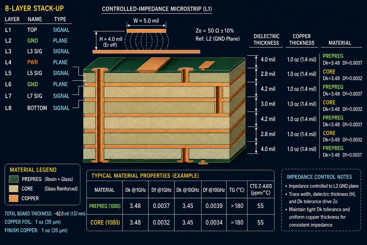
Laminate properties, dielectric thickness and copper geometry work together to determine the electrical behavior of a multilayer PCB.
Material selection cannot be separated from stack-up design.
A multilayer PCB stack-up defines:
For controlled impedance, the distance between the trace and its reference plane is particularly important.
Therefore:
Selecting the laminate after the stack-up has been finalized can create unnecessary redesign work.
Material and stack-up should ideally be developed together.
25. Material Selection and Controlled Impedance
Suppose a designer needs a 50-ohm transmission line.
The required trace width depends on the stack-up.
A simplified relationship is:
Impedance = f(trace width, copper thickness, dielectric thickness, Dk, geometry)
Therefore, if the laminate changes:
Dk changes → impedance changes → trace geometry may need to change
Similarly:
Dielectric thickness changes → impedance changes
This means a laminate substitution should not be treated as a purchasing-only decision.
A material change may require:
26. Can You Substitute One PCB Material for Another?
Sometimes.
But material substitution should not be treated as:
"Both are FR-4, so they are interchangeable."
Before approving a substitution, compare:
For a simple low-speed board, substitution may be relatively straightforward.
For a controlled-impedance or high-reliability board, it may require engineering validation.
27. Material Availability Is Also an Engineering Consideration
A technically excellent material that has long lead times or limited regional availability may create supply-chain risk.
Material selection should therefore consider:
This is particularly important for production programs.
A design should ideally avoid becoming dependent on a material that only one qualified supplier can obtain unless that dependency is intentional and managed.
28. Cost: Why the Cheapest Laminate May Not Be the Cheapest PCB
Material cost is only one component of total PCB cost.
A higher-performance material can affect:
But choosing a cheaper material that cannot reliably meet the electrical or thermal requirement can create much larger downstream costs.
Those costs can include:
Therefore:
Optimize total product risk and cost—not simply laminate purchase price.
29. Can Different Materials Be Used in the Same PCB?
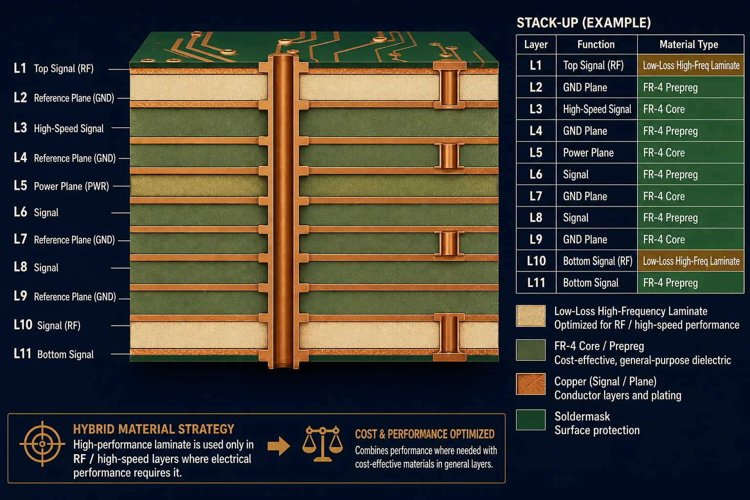
Hybrid PCB constructions can strategically combine conventional and high-performance materials when different parts of the design have different electrical requirements.
Yes.
Hybrid multilayer constructions can combine different dielectric systems when the design requires it.
For example, high-performance dielectric material may be used around:
while more conventional FR-4 materials are used in less electrically demanding portions of the board.
High-frequency material suppliers explicitly support hybrid multilayer constructions combining specialized materials with FR-4 cores and prepregs.
This approach can provide a useful balance between:
Electrical performance + manufacturing practicality + cost
But hybrid construction increases stack-up and fabrication complexity, so it should be engineered deliberately.
30. FR-4 vs High-Tg vs High-Speed vs Specialty Materials
| Material Category | Typical Reason to Consider | Key Properties | Typical Applications |
|---|---|---|---|
| Standard FR-4 | Cost-effective general-purpose PCB | Balanced electrical, mechanical and thermal properties | Industrial, consumer, control electronics |
| High-Tg FR-4 | Greater thermal/reliability margin | Higher Tg, improved thermal capability | Automotive, industrial, high-reliability |
| High-performance FR-4 | Better electrical/thermal balance | Improved Dk/Df, thermal and reliability properties | High-speed digital, demanding multilayer |
| Low-loss high-speed | Signal-integrity requirements | Low Df, controlled Dk | High-speed networking, communications |
| RF/microwave | RF/high-frequency performance | Controlled Dk, low Df, frequency stability | RF, antennas, microwave |
| Specialty thermal materials | Heat-management requirements | Higher thermal conductivity or specialized construction | Power electronics |
| Flexible materials | Flexibility required | Bendability and flexible dielectric construction | Flex circuits, wearable/compact electronics |
Important: These categories overlap. A specific laminate must be evaluated using its manufacturer's published material data and the requirements of the PCB design.
31. Common PCB Material Selection Mistakes
Mistake 1 — Treating all FR-4 as identical
Why it fails:Different FR-4 systems can have significantly different electrical and thermal characteristics.
Mistake 2 — Selecting material solely by Tg
Why it fails:Tg does not define signal loss, impedance behavior, moisture performance or overall reliability.
Mistake 3 — Selecting material only by Dk
Why it fails:Df, tolerance, frequency behavior, temperature stability and construction also matter.
Mistake 4 — Changing laminate without recalculating impedance
Why it fails:Material properties are part of the transmission-line design.
Mistake 5 — Choosing a specialty material because it is "better"
Why it fails:The additional performance may not be required, while cost and manufacturing complexity can increase.
Mistake 6 — Ignoring material availability
Why it fails:A material that cannot be sourced consistently can become a production constraint.
Mistake 7 — Treating material substitution as procurement-only
Why it fails:A laminate change can affect stack-up, impedance, thermal behavior and reliability.
Mistake 8 — Ignoring fabrication compatibility
Why it fails:Some specialty materials require different processing approaches or tighter process control.
Mistake 9 — Ignoring the assembly process
Why it fails:PCB materials experience thermal exposure during assembly and must be compatible with the intended process.
Mistake 10 — Optimizing only for material price
Why it fails:Total manufacturing and product risk can be much more important than laminate cost alone.
32. A Practical PCB Material Selection Workflow
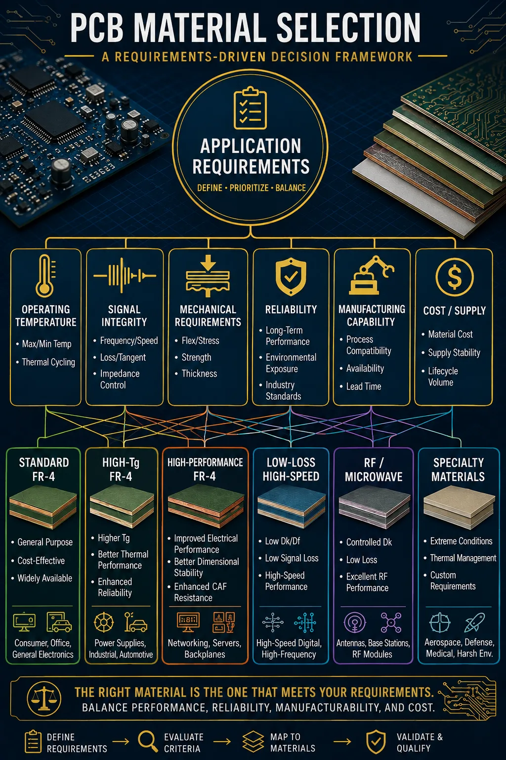
PCB material selection should begin with application requirements and progressively narrow the material choice based on electrical, thermal, mechanical, reliability and manufacturing constraints.
Instead of beginning with:
"Which laminate should we buy?"
start with the product requirements.
Step 1 — Define the operating environment
Determine:
Step 2 — Define electrical requirements
Determine:
Step 3 — Define mechanical requirements
Consider:
Step 4 — Define reliability requirements
Consider:
Step 5 — Define manufacturing requirements
Confirm:
Step 6 — Define commercial requirements
Evaluate:
Step 7 — Build the stack-up
Select:
Step 8 — Validate
Perform:
This process prevents material selection from becoming a last-minute procurement decision.
33. What Information Should Be Specified to the PCB Manufacturer?
For a production PCB, simply specifying:
"FR-4, 1.6 mm"
may be insufficient for a demanding design.
The manufacturing package may need to define, as applicable:
For controlled-impedance designs, the fabricator should have sufficient information to understand the intended stack-up and impedance requirements.
34. How a PCB Manufacturer Can Help With Material Selection
A capable PCB manufacturing partner should be able to discuss more than material availability.
The engineering conversation should include:
Electrical
Thermal
Reliability
Manufacturing
Supply chain
This can be especially valuable when the design is moving from prototype to production.
35. A Material Selection Example
Imagine an industrial controller operating in a relatively demanding environment.
The board has:
The design may not require a specialized RF laminate.
A carefully selected high-performance FR-4 or high-Tg FR-4 family may provide an appropriate balance of:
Thermal reliability + manufacturability + electrical performance + cost
Now consider a second product:
The material decision may move toward a low-loss high-speed laminate.
A third product:
A specialized RF/microwave material may be appropriate.
The lesson is simple:
Material selection should follow the application—not the other way around.
36. PCB Material Selection Checklist
Before releasing a PCB for manufacturing, ask:
Application
Electrical
Thermal
Reliability
Manufacturing
Commercial
Final Engineering Review
37. Engineer's Quick Reference
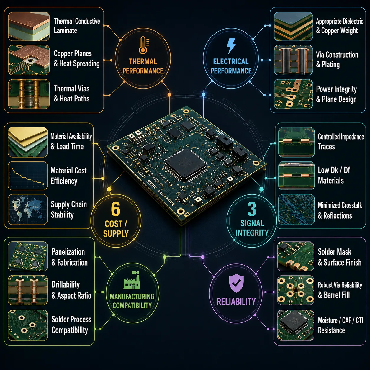
The selected PCB material should be validated across electrical, thermal, mechanical, reliability, manufacturing and commercial requirements before production release.
| Requirement | Material Property to Examine |
|---|---|
| General-purpose PCB | FR-4 family suitability |
| Elevated temperature | Tg, Td, CTE |
| Thermal cycling | Tg, Z-axis CTE, reliability data |
| High-speed digital | Dk, Df, Dk tolerance |
| RF/microwave | Dk, Df, frequency stability |
| Controlled impedance | Dk + dielectric thickness + stack-up |
| High layer count | Z-axis CTE, PTH reliability |
| Humid environment | Moisture absorption, reliability |
| High-density routing | CAF resistance, dimensional stability |
| Lead-free assembly | Thermal/reflow compatibility |
| High-current electronics | Thermal properties + complete board construction |
| Cost-sensitive production | Material availability + fabrication compatibility |
| Hybrid RF/digital design | Hybrid material/stack-up strategy |
38. The Key Principle: Don't Select the Material in Isolation
A PCB material does not exist independently of the rest of the board.
The engineering chain looks like:
Application
↓
Electrical + Thermal Requirements
↓
Material Selection
↓
Stack-Up
↓
Impedance / Signal Integrity
↓
Fabrication Process
↓
Assembly
↓
Reliability
Changing one part can affect the others.
That is why material selection should ideally happen early in the PCB development process.
39. Final Takeaway
FR-4 remains the right answer for a very large number of PCB designs.
The mistake is not using FR-4.
The mistake is assuming that every PCB design needs exactly the same FR-4 material—or that a higher-performance laminate is automatically better.
A practical material-selection strategy is:
Use standard FR-4 when:
The electrical, thermal and reliability requirements are comfortably within its capability.
Consider high-Tg FR-4 when:
The design requires greater thermal margin or reliability under demanding thermal conditions.
Consider high-performance / low-loss materials when:
Signal integrity, insertion loss, impedance control or frequency behavior makes conventional material performance insufficient.
Consider RF/microwave materials when:
The circuit operates at frequencies and electrical requirements where tightly controlled dielectric properties and low loss become critical.
Consider specialty materials when:
The product has unusual thermal, mechanical, environmental or reliability requirements.
The best material is therefore not necessarily the most expensive material.
It is the material that provides the required electrical, thermal, mechanical and reliability performance with adequate manufacturing margin and commercially sustainable supply.
That is the engineering objective.
40. From Material Selection to Production-Ready PCB
Material selection becomes significantly more important when a PCB moves from a prototype into repeat production.
A manufacturing partner should be able to review the relationship between:
For complex or high-performance PCBs, early engineering discussion can prevent a material decision from becoming a late-stage redesign or sourcing problem.
Frequently Asked Questions
Ready to manufacture your electronics project?
Upload your Gerber files & BOM for automated DFM review, engineering feedback, and guaranteed delivery timelines.