PCB Fabrication Process Explained
A Practical Engineering Guide to How Multilayer PCBs Are Manufactured — From CAM Review and Inner-Layer Imaging to Lamination, Drilling, Copper Plating, Surface Finish, Testing, and Final Inspection
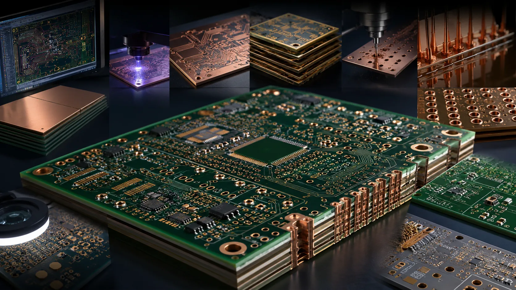
From Engineering Data to a Finished, Tested Printed Circuit Board
Introduction
A PCB may appear to be a relatively simple object: a rigid board containing copper traces, holes, pads and a protective solder mask.
Manufacturing one reliably is anything but simple.
A modern multilayer PCB is produced through a sequence of photolithographic, chemical, mechanical, thermal and electrical processes, with dimensional accuracy and process control required at multiple stages.
The manufacturing route can include:
Engineering review → CAM preparation → material preparation → inner-layer imaging → etching → inspection → lamination → drilling → desmear → copper deposition → plating → outer-layer imaging → pattern plating/etching → solder mask → surface finish → profiling → electrical test → final inspection
The exact sequence changes with the PCB technology.
A conventional two-layer board does not require the same process complexity as an HDI multilayer board.
A high-current board may require different copper construction.
A high-speed board may require tighter control of dielectric construction and impedance.
A rigid-flex board introduces additional material and manufacturing considerations.
So the PCB fabrication process should not be understood as a fixed sequence of identical steps.
It is better understood as a controlled manufacturing flow whose process parameters depend on the board's construction, materials, geometry and performance requirements.
1. The Manufacturing Journey in One View
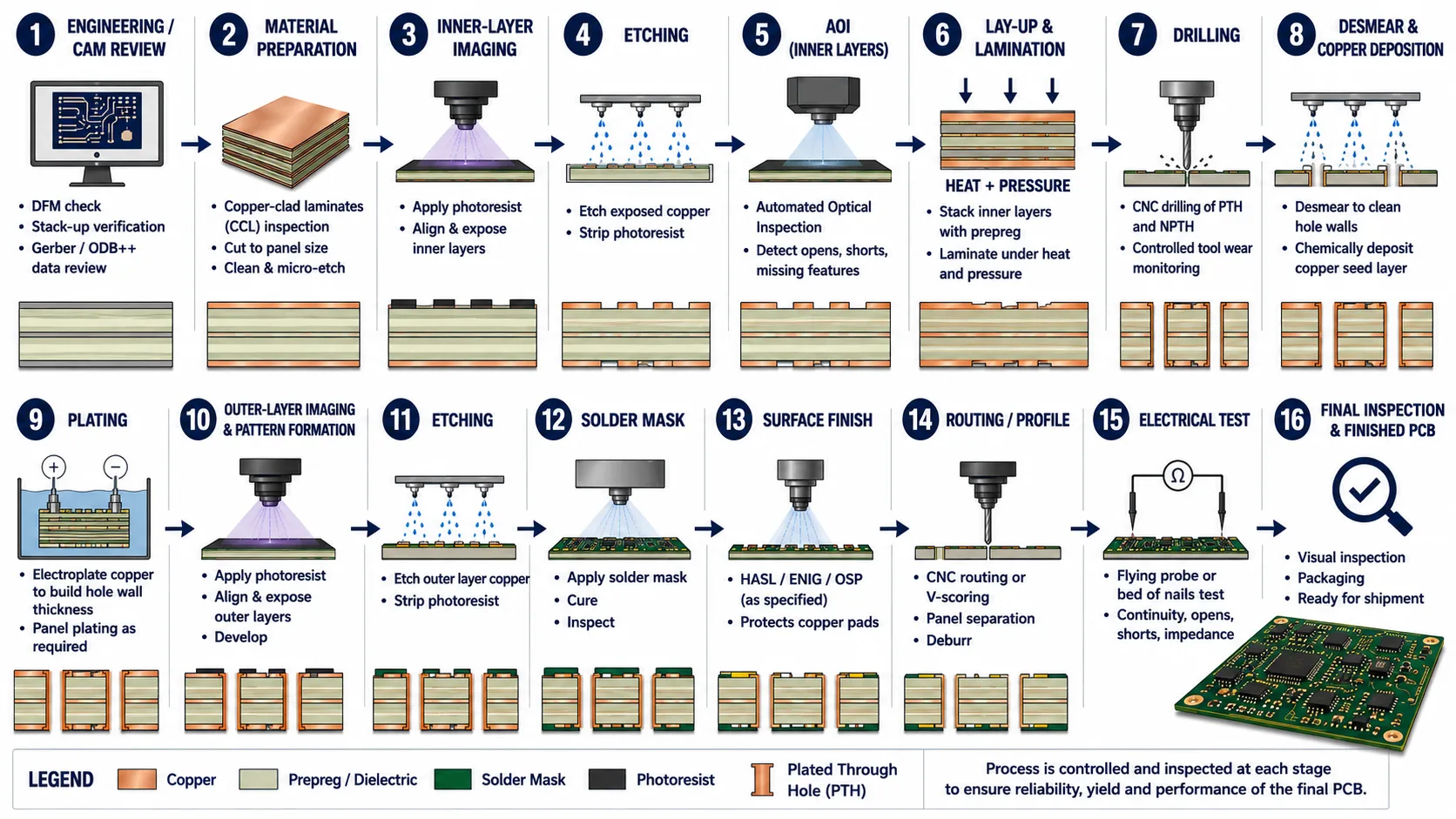
A typical multilayer PCB fabrication flow combines imaging, chemical processing, mechanical operations, plating, surface protection and electrical/visual verification.
At a high level, PCB fabrication converts:
Digital engineering data
into
Physical electrical interconnect
through a controlled sequence of manufacturing operations.
The journey can be simplified into five major phases:
Phase 1 — Engineering Preparation
Phase 2 — Circuit Formation
Phase 3 — Multilayer Construction
Phase 4 — Interconnection and Protection
Phase 5 — Verification and Release
The exact process sequence varies with board construction and technology; multilayer fabrication, for example, introduces inner-layer processing and lamination steps that are not required in the same way for a simple single-sided board.
2. Step 1 — Engineering and CAM Review
PCB fabrication begins before any laminate enters the production process.
The fabricator first needs to translate the customer's manufacturing data into a production-ready process plan.
The engineering/CAM review typically considers:
This stage is critical because manufacturing problems discovered before fabrication are generally much easier to address than problems discovered after panels have entered production.
A CAM engineer may identify issues such as:
The objective is not to redesign the customer's PCB.
The objective is to establish whether the released design data can be translated into a controlled manufacturing process.
3. Why CAM Engineering Matters
A PCB CAD database represents design intent.
The CAM process converts that intent into manufacturing instructions.
That may involve:
This is one of the reasons that a strong PCB manufacturing workflow begins with engineering review rather than immediately starting physical production.
4. Step 2 — Selecting the Base Material
The substrate forms the physical foundation of the PCB.
For many conventional rigid PCBs, FR-4-based laminate systems are widely used.
But “FR-4” should not be treated as a single universal material with identical properties.
Material selection can influence:
For demanding designs, the laminate system may need to be selected according to electrical, thermal and environmental requirements.
IPC identifies IPC-4101 as the specification covering base materials for rigid and multilayer printed boards.
5. Copper Foil and Core Materials
A multilayer PCB is constructed from combinations of:
The copper forms the conductive network.
The dielectric materials provide electrical isolation and establish the physical separation between conductive layers.
The thickness and material properties of these layers influence the final PCB construction.
For high-speed designs, this becomes particularly important because conductor geometry and dielectric geometry are part of the electrical structure.
For power designs, copper thickness and thermal management become significant.
6. Step 3 — Inner Layer Imaging
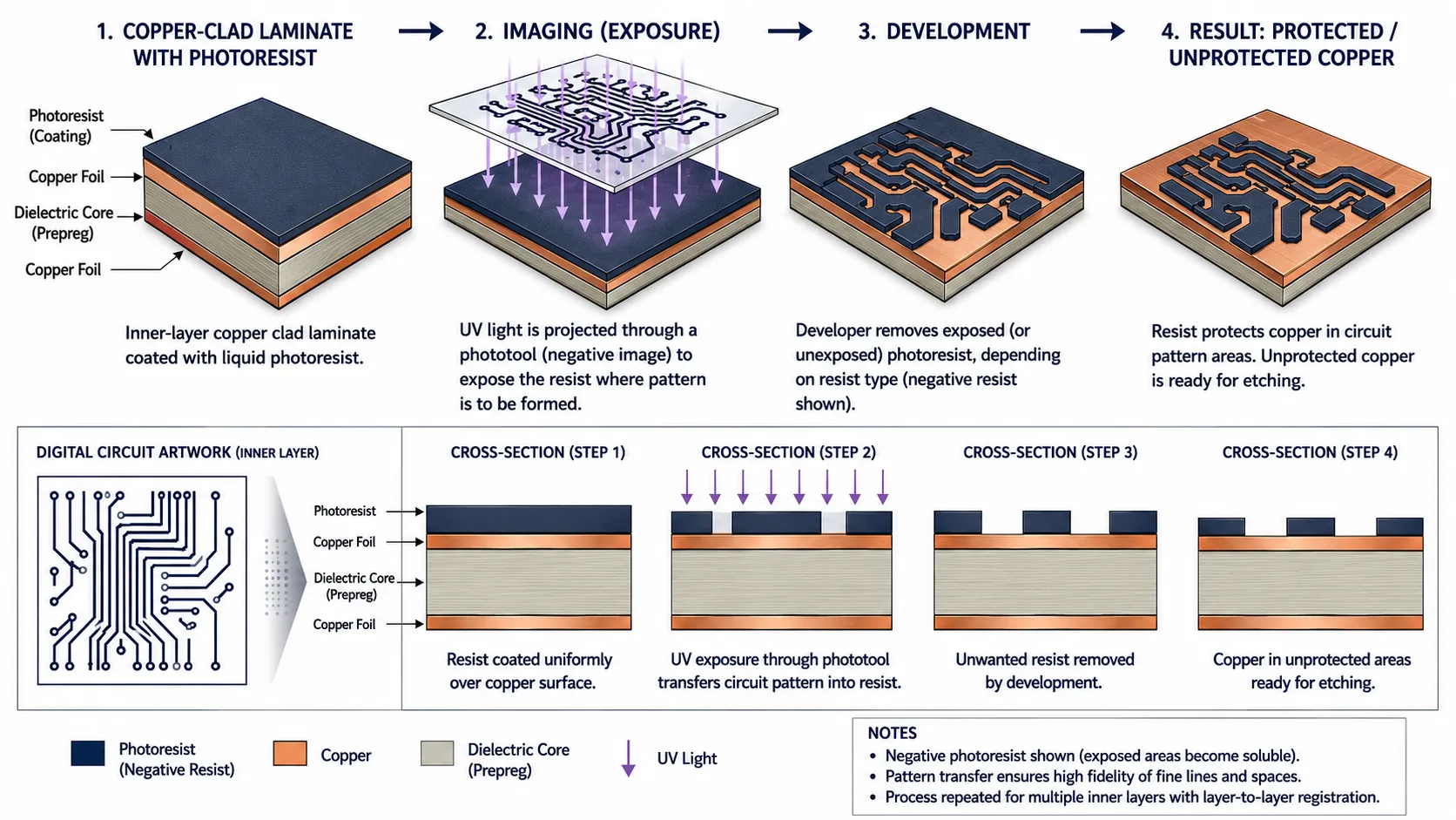
Inner-layer imaging transfers the circuit pattern from manufacturing data onto the copper surface before unwanted copper is removed.
For a multilayer PCB, the inner copper layers must first be formed.
A photosensitive material is applied to the copper surface.
The circuit pattern is transferred onto that surface using imaging equipment.
Modern PCB manufacturing commonly uses direct imaging technologies, although the exact process depends on the manufacturer and board requirements.
The basic objective remains the same:
Transfer the intended copper geometry from digital manufacturing data onto the physical copper layer.
The exposed/non-exposed regions are then developed so that the intended circuit pattern can proceed to the next manufacturing stage.
7. Step 4 — Etching
After imaging and development, unwanted copper is chemically removed.
The protected regions remain as the intended conductive circuitry.
This process is called etching.
The objective is to produce copper traces and planes that match the intended geometry within the required manufacturing tolerances.
Etching therefore directly influences:
The smaller the geometry becomes, the more important process control becomes.
Fine-line PCBs are less forgiving of variations in imaging, resist processing and etching.
8. Why Trace Geometry Can Change During Fabrication
A PCB layout represents nominal geometry.
The fabricated copper is subject to real manufacturing processes.
Etching can remove copper laterally as well as vertically, producing what is commonly referred to as etch compensation or etch factor considerations.
Therefore, fabrication engineering may need to account for process behavior when translating the nominal design into production data.
This is one reason why very fine geometries require careful DFM evaluation.
A design that is electrically correct in CAD is not necessarily equally easy to manufacture at every feature size.
9. Step 5 — Inner-Layer Inspection
Before the inner layers are buried inside the multilayer structure, they should be inspected.
Automated Optical Inspection, or AOI, can be used to compare the manufactured circuit pattern against the intended data.
Typical defect categories can include:
This inspection stage is valuable because an inner-layer defect becomes much more difficult to correct after lamination.
10. Step 6 — Lay-Up and Lamination
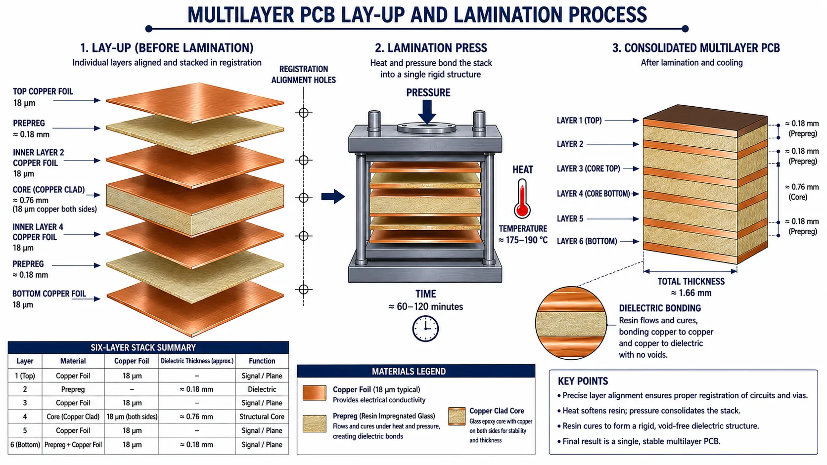
During lamination, individually fabricated layers are accurately aligned and bonded into a single multilayer PCB structure.
Now the individual layers are assembled into a multilayer structure.
The construction may include:
Copper foil → prepreg → core → prepreg → core → prepreg → copper foil
The exact stack-up depends on the board design.
The layers must be accurately aligned before lamination.
Heat and pressure are then applied under a controlled process to bond the structure together.
This creates the solid multilayer PCB panel.
11. Lamination Is More Than “Pressing the Layers Together”
Lamination is a process-control operation.
Parameters such as:
can affect the resulting board.
Poor control can contribute to:
The challenge becomes more significant as the layer count, board thickness, material complexity and dimensional requirements increase.
12. Step 7 — Drilling
Once the multilayer panel has been laminated, holes are created.
Depending on the board technology, drilling may involve:
The resulting structures can include:
Mechanical drilling is widely used for conventional through-holes.
Laser drilling can be used for smaller microvia structures and certain HDI architectures.
The drilling process must maintain accurate:
13. Drill Accuracy and Registration
Drilling is not simply about putting holes through a board.
The hole must land where the electrical and mechanical design requires it to land.
Registration becomes increasingly important in:
Thermal expansion, material behavior and process tolerances can all contribute to registration challenges.
This is one reason that via structure and annular-ring requirements should be considered during PCB design rather than only during fabrication.
14. Step 8 — Desmear and Hole Preparation
After drilling, the hole walls may contain resin smear and other residues generated during the drilling process.
These residues need to be removed or conditioned so that subsequent copper deposition can form a reliable conductive connection.
This stage is generally referred to as desmear.
It is particularly important because the plated hole must ultimately provide electrical continuity between the appropriate copper layers.
The quality of the hole wall directly affects the reliability of the plated-through-hole structure.
15. Step 9 — Electroless Copper and Copper Plating
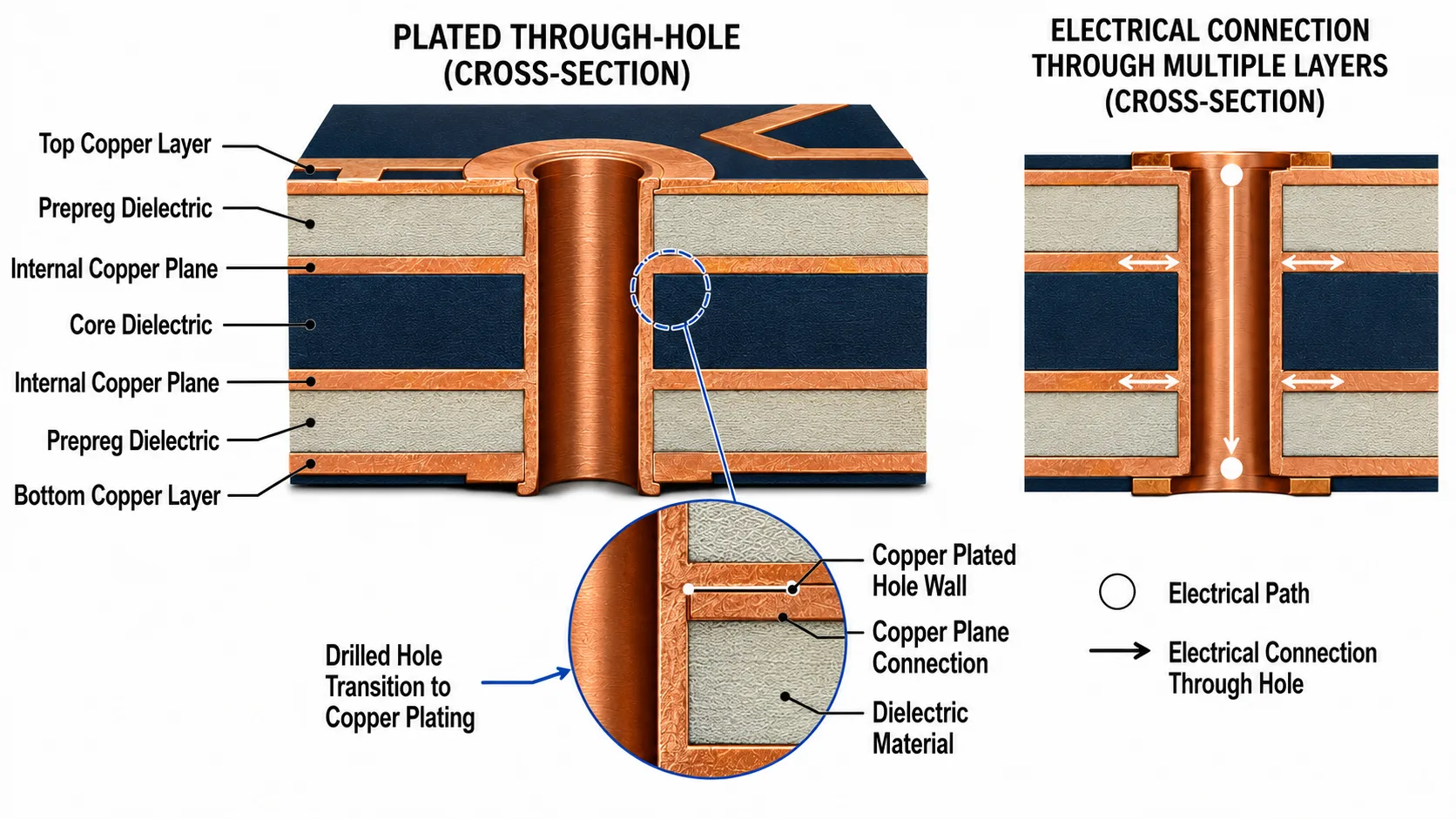
The drilled holes initially do not have the required conductive copper structure.
A conductive copper layer is deposited onto the hole walls, after which electrochemical copper plating builds the required copper thickness.
This creates the electrical interconnection between layers.
The process establishes the conductive path through structures such as:
Top copper → plated barrel → inner copper layer → plated barrel → bottom copper
This is what allows a plated through-hole to electrically connect multiple PCB layers.
16. Why Copper Plating Is a Reliability-Critical Process
The plated hole is exposed to mechanical and thermal stresses throughout the product's life.
During assembly and operation, the PCB can experience repeated temperature changes.
The different materials within the board have different coefficients of thermal expansion.
The plated copper barrel therefore needs sufficient structural integrity to withstand these conditions.
This is why plated-hole quality is not simply a cosmetic concern.
It is a long-term reliability consideration.
IPC-6012 establishes qualification and performance requirements for rigid printed boards, while IPC-A-600 provides acceptability criteria for observable conditions on finished printed boards. IPC explicitly describes these standards as complementary.
17. Step 10 — Outer-Layer Circuit Formation
The outer copper layers now undergo their own imaging and pattern-forming processes.
The objective is to create the final external circuitry including:
Depending on the manufacturing process, copper plating and etching sequences are used to achieve the required conductor pattern and copper thickness.
Outer-layer manufacturing requires careful control because these surfaces will later receive:
18. Step 11 — Outer-Layer AOI
After outer-layer formation, automated optical inspection can again be used to compare the manufactured copper pattern against the intended design data.
The inspection can help detect:
AOI is therefore not simply a final cosmetic inspection.
It is a manufacturing-control mechanism used at appropriate points in the process.
19. Step 12 — Solder Mask
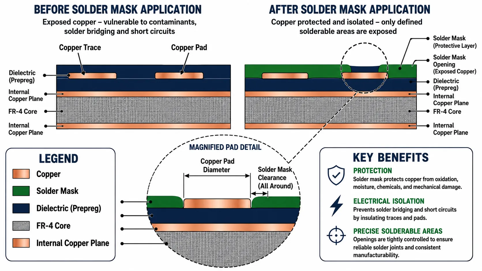
The familiar green—or otherwise colored—protective coating on a PCB is the solder mask.
It serves several important functions.
It helps:
The solder mask is selectively opened over areas such as:
The mask therefore has a functional relationship with the copper geometry beneath it.
20. Step 13 — Surface Finish
Once the PCB has been fabricated, exposed copper pads generally receive a surface finish.
Common finishes include:
The appropriate finish depends on factors such as:
Surface finish should therefore be selected as part of the engineering and manufacturing specification rather than simply as a cosmetic preference.
21. Surface Finish and Assembly
Surface finish affects the interface between the PCB and the soldering process.
For example, fine-pitch and BGA applications can place greater importance on pad planarity.
The surface finish also interacts with:
For this reason, PCB fabrication and PCB assembly should not be treated as completely independent activities.
The bare-board specification needs to support the downstream assembly process.
22. Step 14 — Silkscreen / Legend
The PCB legend provides visual information such as:
The legend does not form part of the electrical circuit.
However, poor legend placement can interfere with pads or reduce assembly readability.
Manufacturing data should therefore define the intended legend appropriately.
23. Step 15 — Board Profiling and Routing
The fabricated PCB panel must eventually be separated into individual boards.
This can involve:
The selected method depends on:
For example, irregular board outlines commonly require routing, while arrays of rectangular boards may use scoring where appropriate.
24. Board Edge Requirements
Some designs place requirements directly on the board edge.
Examples include:
These features should be explicitly documented because they can affect the fabrication route and tooling.
25. Step 16 — Electrical Testing
A PCB may look perfect and still contain an electrical defect.
This is why electrical testing is an important part of the manufacturing process.
Testing can verify conditions such as:
Common approaches include:
Flying Probe Testing
Uses movable probes to access test points.
Advantages can include:
Fixture-Based Testing
Uses a dedicated test fixture to access the required points.
Advantages can include:
The appropriate method depends on the board and production requirements.
26. Electrical Test Is Not the Same as Functional Test
This distinction is important.
Bare-board electrical testing verifies the PCB's electrical interconnections against defined test requirements.
It does not necessarily prove that the completed electronic product performs its intended system function.
Functional testing generally occurs later, after components have been assembled and the complete electronic assembly is available.
So:
PCB fabrication test ≠ PCBA functional test
This distinction should be clear when defining manufacturing requirements.
27. Step 17 — Final Inspection
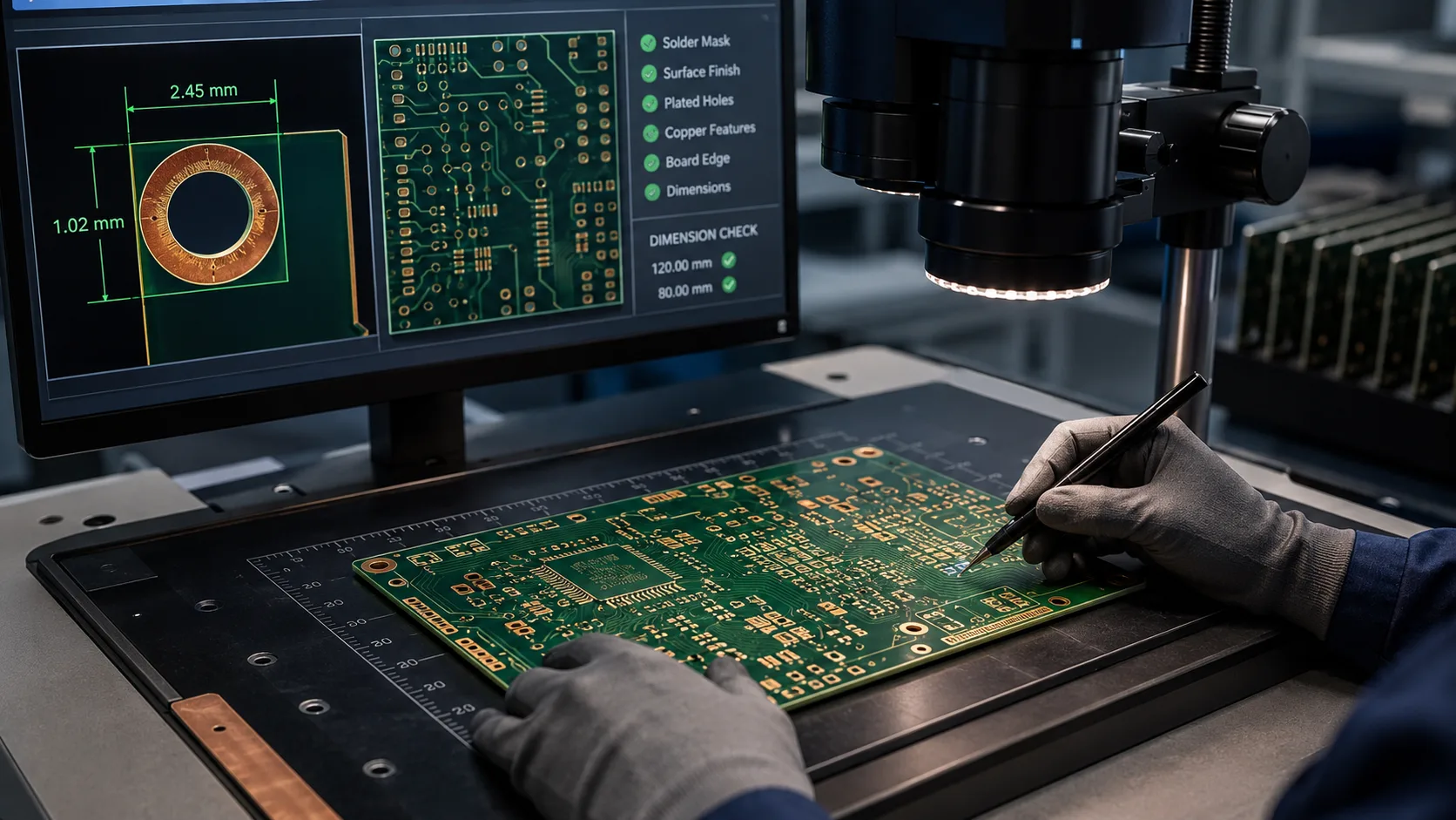
Before shipment, the finished PCB undergoes final inspection.
Depending on the product and specification, inspection can cover:
IPC-A-600 provides illustrated acceptability guidance for printed boards, including target, acceptable and nonconforming conditions. IPC states that it is intended to work together with the applicable performance specifications such as IPC-6012.
28. Where IPC Standards Fit Into the Fabrication Process
IPC standards should not be treated as a single “quality certificate” attached to a PCB.
Different IPC documents address different aspects of design, fabrication, performance and acceptability.
For example:
IPC-2221
Provides generic PCB design requirements and principles. IPC identifies it as the generic design standard forming the basis of the IPC-2220 series.
IPC-6012
Defines qualification and performance requirements for rigid printed boards. IPC's current standards information lists IPC-6012F for rigid printed boards.
IPC-A-600
Provides visual acceptability criteria for printed boards, including target, acceptable and nonconforming conditions.
IPC-TM-650
Provides recognized test methods for various PCB-related electrical, chemical, mechanical and environmental evaluations.
The important engineering principle is:
The applicable standard, revision, product class and customer specification should be explicitly defined rather than assuming that “IPC compliant” means the same thing for every PCB.
29. Product Class Matters
Not every PCB has the same reliability requirement.
The acceptable manufacturing condition for a low-risk prototype may not be appropriate for a high-reliability product.
Product classification therefore matters.
The customer and manufacturer should establish the applicable requirements and acceptance criteria before production.
This becomes particularly important for applications such as:
For these applications, the relevant specification may include additional customer, regulatory, industry or application-specific requirements beyond a generic PCB fabrication specification.
30. What Happens When the PCB Is High-Density?
The fabrication process becomes increasingly demanding as PCB density increases.
Consider an HDI board with:
The manufacturer must control:
IPC identifies IPC-2226 as the sectional design standard for HDI printed boards.
The key lesson is:
Increasing electrical density increases manufacturing-process sensitivity.
That is why HDI decisions should be considered during design and DFM—not after the board has already been released.
31. Controlled Impedance Changes the Manufacturing Conversation
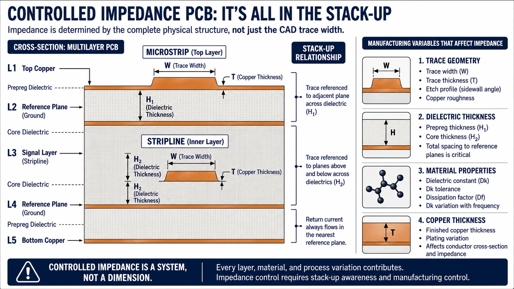
For high-speed boards, the PCB is part of the electrical transmission system.
Trace geometry alone does not define impedance.
Impedance depends on relationships involving:
IPC identifies IPC-2141 as a design guide for controlled-impedance circuit boards and high-speed logic design.
Therefore, an impedance requirement should be communicated as part of the manufacturing definition.
The fabricator needs enough information to establish and control the intended structure.
32. How Fabrication Decisions Affect Cost
PCB cost is not determined by board area alone.
Manufacturing cost can be influenced by:
This is why two boards with similar dimensions can have significantly different manufacturing costs.
A sourcing manager should therefore compare quotations against the same technical construction.
33. Manufacturing Yield Is a Design Consideration
Suppose two PCB designs perform identically from an electrical standpoint.
One uses:
The other uses:
Both may be technically manufacturable.
But they do not necessarily have the same:
This is the essence of Design for Manufacturability.
The objective is not merely to create something that can be manufactured.
The objective is to create something that can be manufactured consistently and economically at the required quality level.
34. Engineering Review Before Fabrication
A strong PCB fabrication workflow therefore begins well before the first manufacturing process.
The supplier should understand:
Electrical requirements
Mechanical requirements
Material requirements
Manufacturing requirements
Quality requirements
35. A Practical Fabrication Readiness Checklist
Before releasing a PCB for fabrication:
Manufacturing Data
☐ Gerber or approved fabrication data☐ NC drill data☐ Board outline☐ Fabrication drawing☐ Stack-up☐ Revision identification
Construction
☐ Layer count☐ Material☐ Finished thickness☐ Copper thickness☐ Surface finish
Electrical
☐ Controlled impedance requirements☐ Electrical test requirements☐ Special electrical features
Mechanical
☐ Board dimensions☐ Hole sizes☐ Slots☐ Cut-outs☐ Edge requirements
DFM
☐ Minimum trace/space reviewed☐ Annular ring reviewed☐ Drill capability reviewed☐ Copper-to-edge clearance reviewed☐ Solder-mask requirements reviewed☐ HDI requirements reviewed where applicable
Quality
☐ Applicable IPC/customer requirements identified☐ Inspection requirements defined☐ Test requirements defined☐ Acceptance criteria understood
36. A Representative Engineering Scenario
When a “Standard” PCB Wasn't Actually Standard
Consider a four-layer controller PCB intended for industrial equipment.
The board initially appears straightforward.
However, engineering review identifies:
The board is technically manufacturable.
But the manufacturing requirements are not equivalent to a generic four-layer FR-4 board.
The fabricator must consider:
The lesson is important:
Board complexity is determined by manufacturing and performance requirements—not simply by layer count.
A four-layer board can be straightforward.
Another four-layer board can require significantly more process control.
37. What a Sourcing Manager Should Ask a PCB Supplier
A procurement professional does not need to become a PCB process engineer.
But several questions can materially improve supplier evaluation.
Ask:
These questions help move procurement from:
“Who gives me the cheapest PCB?”
to:
“Who is quoting the same technical product against a controlled manufacturing specification?”
That is a much stronger basis for supplier comparison.
38. Why Engineering-to-Manufacturing Handoff Matters
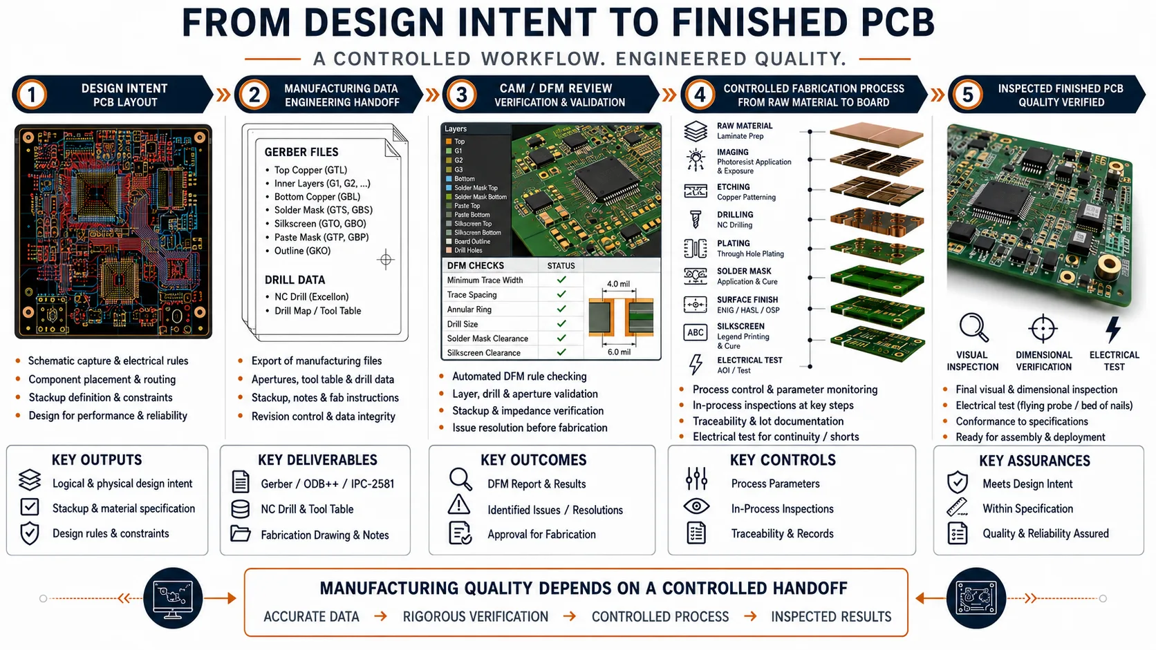
The PCB fabrication process is ultimately a chain of translations:
Design intent
↓
Manufacturing data
↓
CAM interpretation
↓
Physical process parameters
↓
Finished PCB
Every transition introduces the possibility of interpretation or process variation.
A strong manufacturing partner therefore adds value not only through fabrication equipment, but through the engineering discipline surrounding the fabrication process.
39. How QUADRIONIX Approaches the Manufacturing Transition
For a PCB manufacturing project, the objective should be to establish a clear technical path from customer design data to production.
A disciplined workflow can be represented as:
Customer Manufacturing Package
↓
Engineering / DFM Review
↓
Manufacturing Specification Confirmation
↓
Fabrication Planning
↓
PCB Production
↓
Inspection & Electrical Test
↓
Final Release
This approach is particularly useful when customers are sourcing internationally and need confidence that the supplier understands the engineering requirements behind the files.
For projects that continue into PCB assembly or turnkey PCBA, the process can then extend into:
PCB Fabrication → Component Sourcing → SMT/THT Assembly → Inspection → Testing → Production Readiness
The objective is to reduce the gap between what the customer designed and what ultimately gets manufactured.
40. PCB Fabrication Is a System, Not a Single Process
The biggest misconception about PCB manufacturing is that fabrication is simply:
Copper + drilling + etching = PCB.
In reality, reliable fabrication depends on the interaction of:
A defect introduced at one stage can affect downstream manufacturing.
A registration error can affect drilling.
A drilling problem can affect plating.
A plating problem can affect reliability.
A poor surface finish can affect assembly.
An incomplete manufacturing specification can affect the entire production process.
This is why PCB manufacturing must be viewed as an integrated process chain.
41. Key Takeaways
1. PCB fabrication starts with engineering data—not with laminate.
The quality of the manufacturing release influences the quality of the manufacturing process.
2. Multilayer PCBs require controlled layer registration.
Lamination and drilling accuracy become increasingly important as board density increases.
3. Copper plating is fundamental to electrical interconnection.
Plated-through-hole reliability is an important part of PCB performance.
4. Solder mask and surface finish are functional manufacturing steps.
They influence protection, solderability and downstream assembly.
5. Electrical testing and visual inspection serve different purposes.
A board can pass visual inspection and still require electrical verification.
6. IPC standards need to be applied appropriately.
Design requirements, performance specifications and acceptability criteria address different parts of the manufacturing system.
7. DFM should happen before production.
The best manufacturing problem is one identified before the board enters production.
8. The cheapest quotation is not automatically the lowest-cost manufacturing solution.
Material, construction, process capability, yield, testing and reliability all contribute to the real cost.
42. Conclusion
A printed circuit board is the physical result of a highly coordinated manufacturing process.
The journey begins with digital engineering data and passes through:
CAM review → material preparation → imaging → etching → inspection → lamination → drilling → desmear → copper plating → outer-layer formation → solder mask → surface finish → profiling → electrical testing → final inspection.
Each stage has a specific purpose.
Each stage also introduces manufacturing variables that can influence the final product.
For engineers, understanding this process helps explain why certain PCB design decisions matter.
For sourcing managers, it provides a framework for asking better questions and comparing suppliers on technical equivalence rather than price alone.
For product teams, it helps connect the design office to the factory floor.
And for an international manufacturing program, that connection becomes particularly important.
A PCB is not manufactured from artwork alone. It is manufactured from engineering intent translated into controlled materials, processes, tolerances, inspections and acceptance criteria.
That is the foundation of reliable PCB fabrication.
Frequently Asked Questions
Ready to manufacture your electronics project?
Upload your Gerber files & BOM for automated DFM review, engineering feedback, and guaranteed delivery timelines.