How to Prepare PCB Manufacturing Files Correctly
A Practical Guide to Gerber Files, Drill Data, Stack-Up, Fabrication Drawings, CAM Validation and Controlled Manufacturing Release
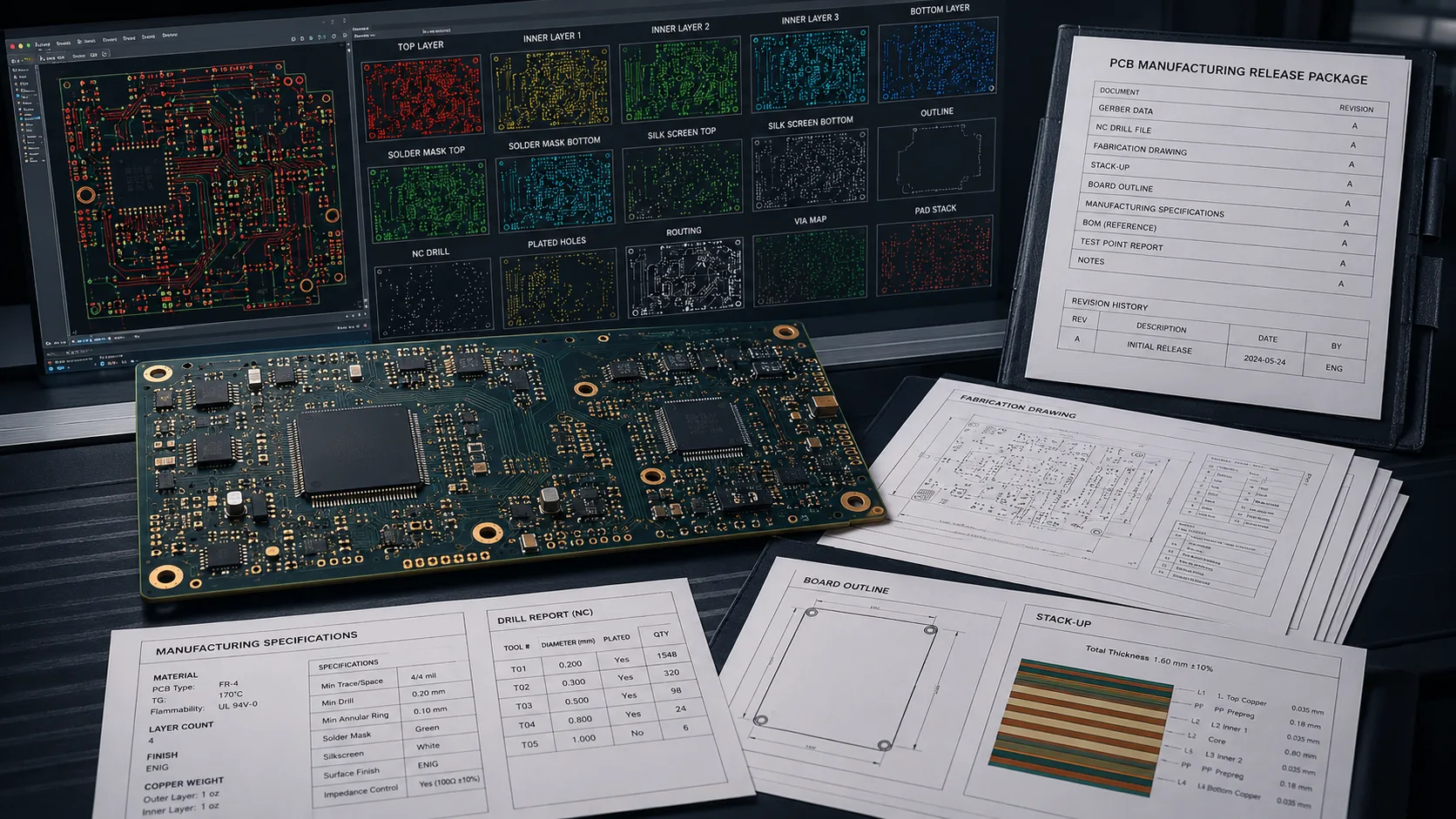
A PCB design can be electrically correct, mechanically correct and fully routed—and still not be ready for manufacturing.
That distinction is important.
The CAD database contains the designer's engineering intent. A PCB fabricator, however, needs a manufacturing definition that clearly communicates:
what needs to be built,
how the board is constructed,
where every manufacturing feature is located,
what materials and finishes are required,
what tolerances apply,
how the finished board should be verified,
and which revision is authorized for production.
A manufacturing package therefore needs to answer questions such as:
How many copper layers does the board have?
What is the finished board thickness?
What copper thickness is required?
What material system should be used?
What is the final board outline?
Where are the holes?
Which holes are plated?
Which holes are mechanical?
What surface finish is required?
Is controlled impedance required?
What dimensional tolerances apply?
Are there special fabrication requirements?
What inspection and electrical testing are expected?
Which revision is the current release?
If these answers are incomplete, contradictory or ambiguous, the fabricator may have to make assumptions.
That is where avoidable manufacturing risk begins.
A professional PCB manufacturing package should therefore be treated as a controlled engineering release, not simply as a ZIP file containing exported Gerbers.
1. What Is a PCB Manufacturing Package?
A PCB manufacturing package is the collection of manufacturing files, drawings and specifications required by the fabricator to manufacture the bare PCB according to the intended design.
Depending on the board and supplier, it may include:
Fabrication Data
Gerber or equivalent manufacturing data
NC drill files
Board outline/profile
Slots and cut-outs
Mechanical features
Construction Information
Layer stack-up
Material specification
Copper thickness
Finished board thickness
Dielectric information
Controlled-impedance requirements
Manufacturing Specifications
Surface finish
Solder-mask requirements
Silkscreen/legend
Special fabrication requirements
Manufacturing notes
Electrical-test requirements
Quality and Release Information
Applicable standards
Product classification
Acceptance criteria
Customer-specific requirements
Part number
Revision
Release information
The exact package depends on the technology.
A simple two-layer prototype may require a relatively straightforward package.
An HDI, high-layer-count, controlled-impedance or rigid-flex board may require substantially more manufacturing definition.
2. Gerber Files vs the Complete Manufacturing Package
This is one of the most important concepts in the article.
Gerbers are not the entire manufacturing specification.
Gerber files primarily communicate PCB artwork geometry.
The complete manufacturing definition may additionally require:
drill data
board outline
fabrication drawing
stack-up
materials
copper thickness
finished thickness
surface finish
impedance requirements
quality requirements
testing requirements
special manufacturing instructions
revision information
The first source explicitly makes this distinction, while the Gerber-focused article reinforces that Gerbers form the core of a package but do not necessarily communicate the complete physical construction.
The better question is not:
“Did I export the Gerbers?”
It is:
“Could an experienced fabricator manufacture the intended PCB from this package without making an assumption?”
That is the stronger test.
3. Native PCB Design Files vs Manufacturing Files
A native CAD project may contain:
schematics
component libraries
design rules
net information
routing
constraints
layer definitions
component placement
3D models
manufacturing settings
internal CAD metadata
The fabricator does not necessarily need all of this information to manufacture the bare board.
Instead, the design is translated into manufacturing output:
Native PCB Design
↓
Manufacturing Output Configuration
↓
Gerber / ODB++ / IPC-2581 / Equivalent
↓
NC Drill
↓
Fabrication Drawing
↓
Manufacturing Specifications
↓
CAM / Engineering Review
↓
PCB Fabrication
The important point is that exporting manufacturing files is a translation step. A correct CAD design can still produce an incomplete or incorrectly configured manufacturing package if the export configuration is wrong.
4. Gerber, ODB++ or IPC-2581?
There is no universal requirement that every PCB project use only Gerber.
Depending on the design workflow and supplier, manufacturing data may be exchanged using:
Gerber
ODB++
IPC-2581
other supplier-supported formats
Gerber remains widely used and understood.
ODB++ and IPC-2581 can provide richer structured manufacturing information.
The important principle is:
The manufacturing data must accurately and unambiguously represent the intended PCB construction.
The selected format should therefore be confirmed with the intended fabricator before release.
5. Start With the Correct Design Revision
Before generating manufacturing files, freeze the correct design revision.
Verify:
PCB revision
schematic revision
BOM revision where applicable
component library revision where relevant
mechanical revision
manufacturing notes
engineering-change status
If the PCB changes after Gerber generation, the previous Gerber package should not automatically be assumed to remain valid.
A controlled release should establish exactly which design revision the manufacturing files represent.
6. What Does a Typical Gerber Package Contain?
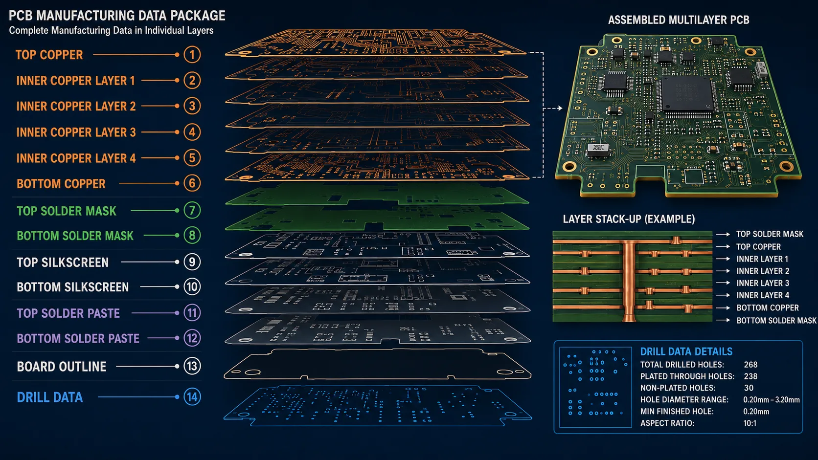
A PCB manufacturing package translates the design into defined fabrication layers, drilling data, board geometry and manufacturing requirements.
A conventional multilayer PCB may contain:
Manufacturing Data | Typical Purpose |
|---|---|
Top Copper | Conductors, pads, routing and copper pours |
Inner Copper Layers | Internal signal/plane layers |
Bottom Copper | Bottom-side conductors and pads |
Top Solder Mask | Top mask openings |
Bottom Solder Mask | Bottom mask openings |
Top Silkscreen | References and markings |
Bottom Silkscreen | Bottom-side markings |
Top Paste | SMT stencil data |
Bottom Paste | Bottom-side stencil data where applicable |
Board Outline | Finished board geometry |
Drill Data | Hole locations and sizes |
Not every PCB requires every layer.
The exact file set depends on the board configuration and manufacturing process.
7. Verify Every Required Copper Layer
For a multilayer board, every intended copper layer must be represented.
For example, a four-layer board normally requires:
Top Copper
Inner Copper 1
Inner Copper 2
Bottom Copper
A six-layer board requires the corresponding six copper artwork layers.
Before release:
Number of copper layers in the design = number of copper layers in the manufacturing package.
Also verify the layer order.
A swapped inner layer can fundamentally change the manufactured PCB.
8. Use Clear and Consistent Layer Identification
File naming can appear administrative, but it has practical manufacturing value.
A package containing:
Layer1
Layer2
Layer3
Layer4
is less immediately understandable than one where the functional identity of each file is clear.
The exact naming convention can vary.
The goal is:
The manufacturer should be able to determine what every file represents without guessing.
At minimum, the package should clearly identify:
top copper
inner copper
bottom copper
solder mask
silkscreen
paste
outline
drill data
A layer-mapping table can be especially useful.
9. Verify Solder-Mask Layers
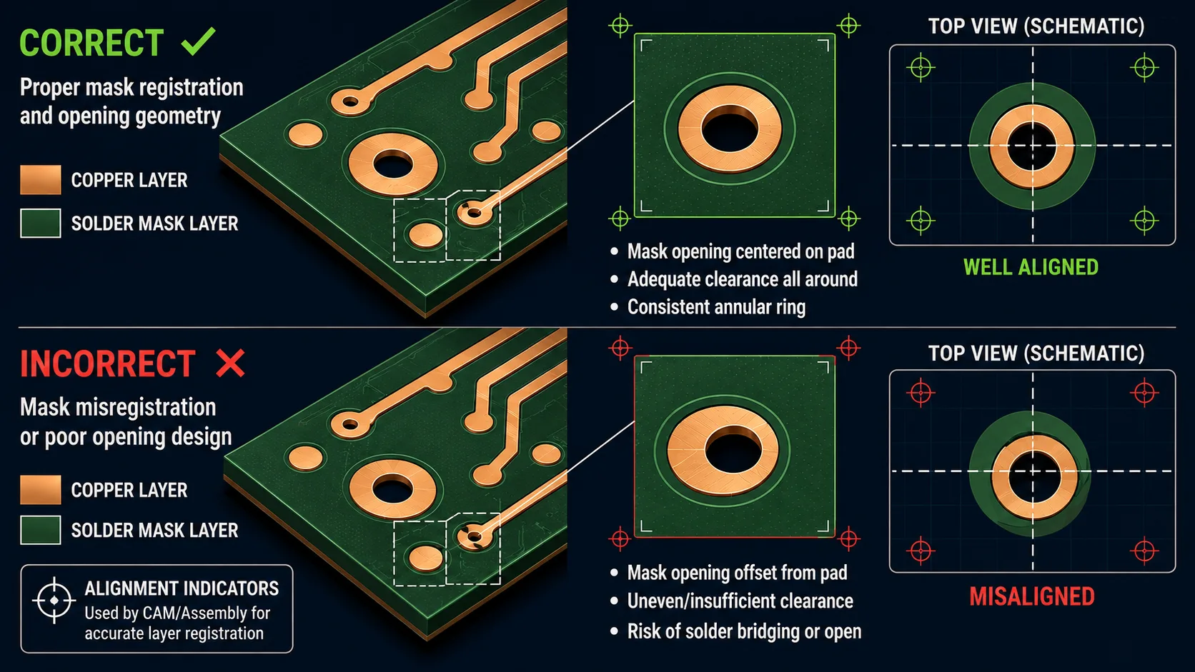
Solder-mask openings must correctly correspond to the underlying copper features.
Solder-mask files define where protective solder mask is opened.
Typically:
Top Solder Mask
Bottom Solder Mask
The openings must correspond correctly with pads and other exposed features.
Check for:
missing openings
unintended openings
incorrect pad exposure
solder-mask slivers
mask expansion problems
copper/mask mismatch
Particular attention is required around:
fine-pitch components
BGA pads
thermal pads
test points
high-voltage clearances.
10. Check Silkscreen and Legend
Silkscreen may contain:
reference designators
polarity indicators
connector labels
component outlines
revision markings
warning labels
identification markings
Check for overlap with:
component pads
exposed copper
board edges
mounting holes
critical markings
A reference designator can technically exist in the file while being unusable on the physical PCB if it ends up underneath a component or over a solderable pad.
Silkscreen is therefore part of the board's usability and identification system, not merely decorative artwork.
11. Board Outline: One of the Most Critical Manufacturing Files
The board outline defines the finished physical boundary of the PCB.
It may include:
outer perimeter
internal cut-outs
slots
mechanical holes
edge features
breakaway features
V-score requirements
routed edges
unusual contours
The outline must be unambiguous.
One common failure is having multiple mechanical layers containing apparently different versions of the board shape.
The fabricator should never have to guess which geometry defines the finished PCB.
12. Internal Cut-Outs and Slots
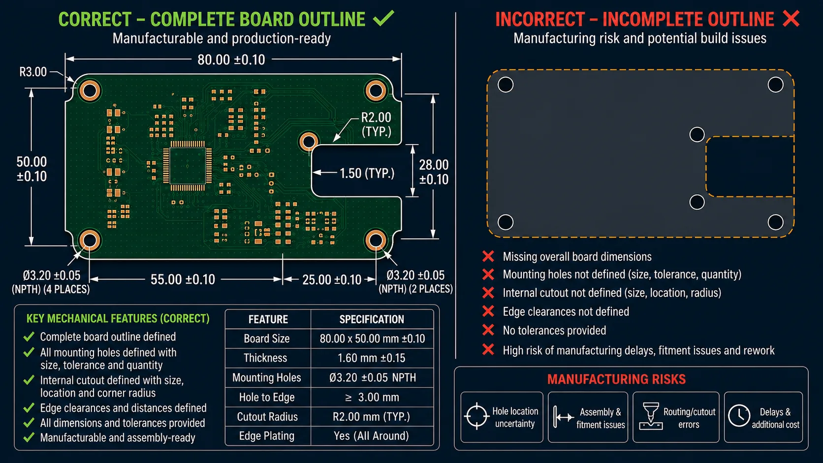
The board outline must accurately represent the intended finished PCB geometry, including cut-outs and special edge features.
Internal openings may be required for:
connectors
mounting interfaces
batteries
displays
chassis interfaces
antenna regions
A slot also needs to be distinguished from a conventional drilled hole.
For example:
Circular hole → drill
Long slot → routed/mechanical feature
The exact manufacturing implementation depends on the fabricator, but the intended manufacturing function needs to be clear.
13. Generate and Validate NC Drill Data
The NC drill file communicates hole locations and sizes.
Depending on the design, it may contain:
plated holes
non-plated holes
vias
mounting holes
tooling holes
mechanical holes
Review:
hole count
tool diameters
hole locations
plated/non-plated intent
finished versus drilled diameter where applicable
hole tolerances
slots or routed holes
Drill data should always be checked against the copper artwork rather than treated as an independent file.
14. Finished Hole Size vs Drill Tool Size
This is an important engineering distinction.
The specified finished hole diameter is not necessarily the same as the drill-tool diameter.
Manufacturing processes can introduce dimensional changes between drilling and the finished plated hole. For plated holes, copper deposition affects the internal diameter.
The fabricator's CAM process may therefore apply appropriate manufacturing compensation.
For this reason:
Do not casually edit drill files manually to “fix” hole sizes.
The intended finished-hole requirement should instead be clearly communicated in the manufacturing specification.
15. Plated vs Non-Plated Holes
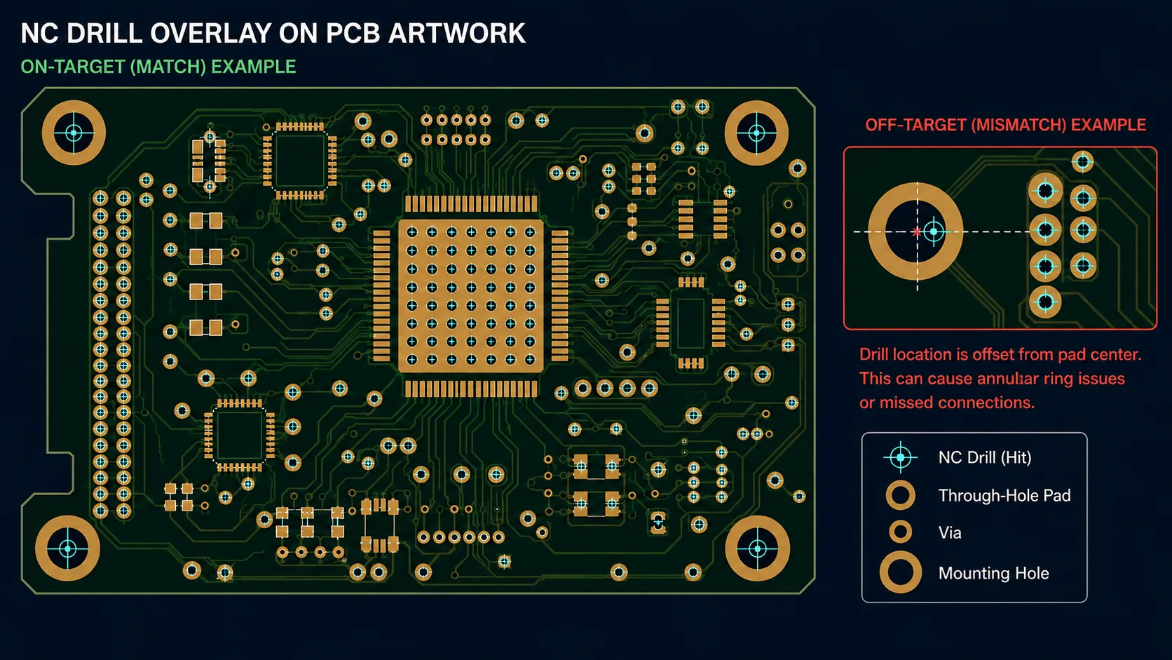
The manufacturing package should clearly distinguish:
Plated Through-Holes
Potentially used for:
component leads
electrical interconnection
through-hole vias
certain electrical/mechanical features
Non-Plated Through-Holes
Often used for:
mounting
mechanical clearance
chassis interfaces
tooling
Confusing these two can create a significant manufacturing problem.
16. The Fabrication Drawing
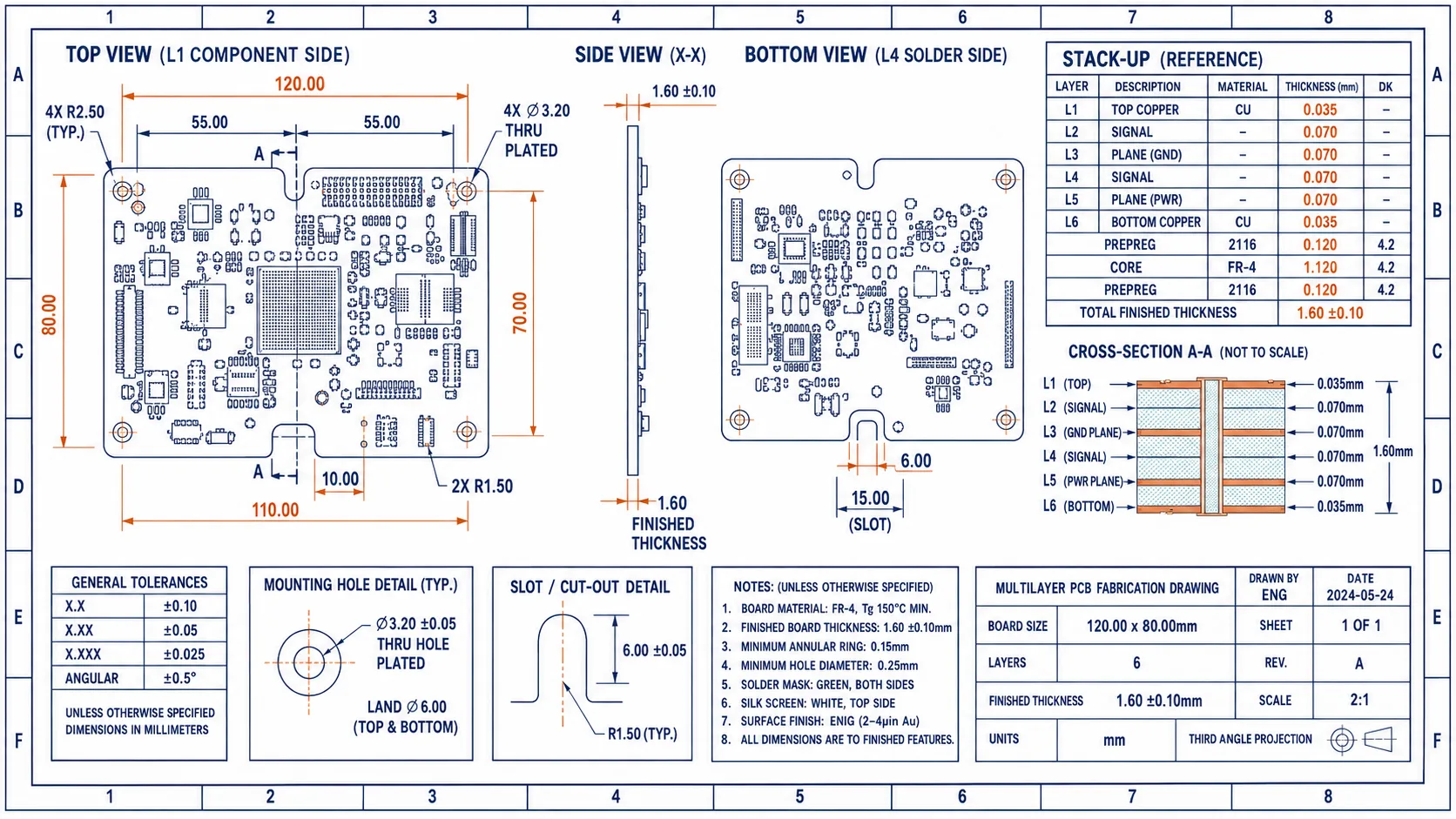
A fabrication drawing is one of the most valuable documents in a professional manufacturing package.
It can communicate information that may not be obvious from Gerber and drill data alone.
Typical information includes:
board dimensions
finished thickness
layer count
material
copper thickness
surface finish
tolerances
hole requirements
controlled impedance
special notes
revision
manufacturing standards
electrical-test requirements
The fabrication drawing therefore acts as both a manufacturing specification and engineering reference document.
17. Define the Physical Stack-Up
For multilayer PCBs, the stack-up is fundamental.
It defines the physical arrangement of:
copper layers
core materials
prepreg
dielectric layers
copper foil
It can also define:
dielectric thickness
copper thickness
finished board thickness
reference planes
controlled-impedance structures
A stack-up should not be left ambiguous when electrical performance depends upon it.
18. Gerber Layers Are Not the Physical Stack-Up
This distinction is particularly important for multilayer and high-speed boards.
Gerber artwork describes layer geometry.
The physical stack-up defines how those layers are actually constructed.
For example, a four-layer design may have:
L1 → L2 → L3 → L4
But that alone does not define:
dielectric thickness
copper thickness
reference-plane distance
material properties
finished thickness
Those physical parameters can affect electrical performance.
Therefore:
Gerber artwork and physical stack-up must be considered together.
19. Controlled Impedance Requirements
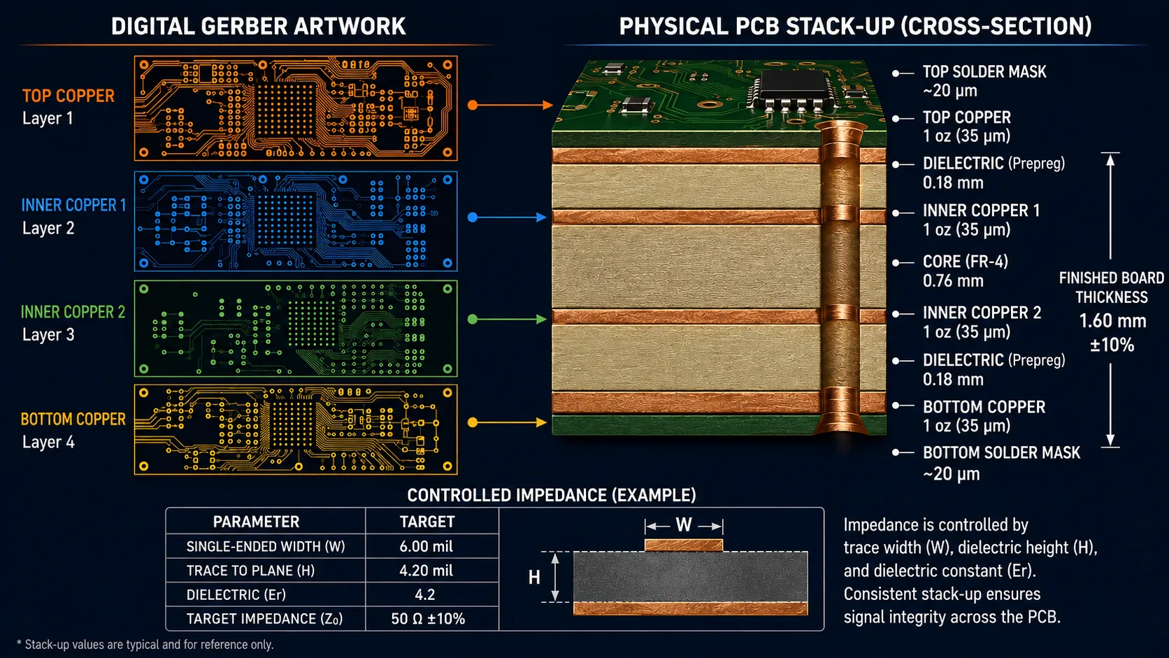
For controlled-impedance designs, specify:
target impedance
applicable signal structures
tolerance where required
relevant layers
reference planes
required impedance coupons or verification where applicable
For example:
50 Ω single-ended
90 Ω differential
But simply stating the impedance target is not enough.
Impedance depends on:
trace width
trace thickness
dielectric thickness
dielectric properties
reference-plane location
surrounding geometry
Therefore:
Controlled impedance is a system-level manufacturing requirement, not simply a Gerber-layer requirement.
20. Material Specification
Avoid overly vague specifications such as:
“Use FR-4.”
FR-4 describes a broad class of materials rather than one identical laminate system.
Depending on the application, the specification may need to address:
laminate family
Tg
Dk/Df where relevant
thermal requirements
copper foil
thickness
special material requirements
For high-frequency applications, conventional FR-4 assumptions may not be sufficient.
For demanding thermal applications, laminate and copper construction may also require additional consideration.
21. Finished Board Thickness
Specify:
nominal finished thickness
applicable tolerance
This can matter for:
mechanical fit
connector interfaces
chassis integration
thermal/mechanical design
assembly
reliability
A nominal thickness without a tolerance can leave room for interpretation, particularly where mechanical integration is tight.
22. Copper Thickness
Copper thickness affects:
current-carrying capability
resistance
thermal performance
trace geometry
fabrication process
cost
A high-current board may require heavier copper.
However, heavier copper can also make fine-feature fabrication more difficult.
This is an important engineering trade-off:
More copper can improve current capability—but can reduce fine-feature manufacturability.
23. Surface Finish
The manufacturing package should specify the required surface finish.
Common options include:
ENIG
ENEPIG
HASL / lead-free HASL
OSP
immersion silver
immersion tin
The choice can affect:
solderability
pad planarity
fine-pitch assembly
storage
reliability
cost
The finish should therefore be specified rather than left to an undefined supplier assumption.
24. Solder Mask and Silkscreen Requirements
The manufacturing specification should define relevant solder-mask requirements such as:
top/bottom mask
mask color where relevant
mask openings
via tenting
critical pad clearances
Particular attention may be needed around:
BGA pads
fine-pitch components
thermal pads
test points
high-voltage areas
Silkscreen should similarly define required identification and markings.
25. Trace Width, Spacing and Fabrication Capability
The manufacturing package should reflect the intended design geometry.
Important parameters include:
minimum trace width
minimum spacing
copper-to-edge clearance
pad-to-pad spacing
via-to-via spacing
via-to-pad spacing
These interact with:
layer count
copper thickness
material
fabrication process
yield
cost
Therefore, the PCB should be evaluated against the actual fabricator's capability, rather than generic “minimum capability” values found online.
A manufacturing file package should communicate the design clearly, but the design itself must still be checked for manufacturability.
26. Annular Rings and Advanced Via Technology
The manufacturing package should make the required via technology clear.
Potential structures include:
through vias
blind vias
buried vias
microvias
via-in-pad
Annular-ring requirements are influenced by:
pad diameter
drill diameter
registration
plating
manufacturing tolerances
Advanced via technologies can significantly affect fabrication complexity and cost.
For via-in-pad, additional treatment may be required depending on the design, such as:
filling
capping
planarization
The intended requirement should be explicit rather than left for the fabricator to interpret.
27. Electrical Test Requirements
If bare-board electrical testing is required, define it in the manufacturing specification.
Potential requirements include:
continuity
isolation
opens
shorts
test coverage
test method
For higher-volume production, fixture-based testing may be appropriate.
For prototypes or lower-volume production, flying-probe testing may offer greater flexibility.
The correct approach depends on the production program.
28. Quality and Acceptance Requirements
A manufacturing package should identify applicable quality requirements.
These may include:
applicable IPC performance specification
product class
customer-specific requirements
inspection requirements
electrical testing
special reliability testing
acceptance criteria
The source article specifically notes the importance of distinguishing between an applicable performance specification and visual acceptability criteria rather than simply stating:
“PCB must meet IPC standards.”
The release should identify the applicable specification, product class, acceptance criteria and customer-specific requirements where applicable.
29. Revision Control: The Silent Manufacturing Risk
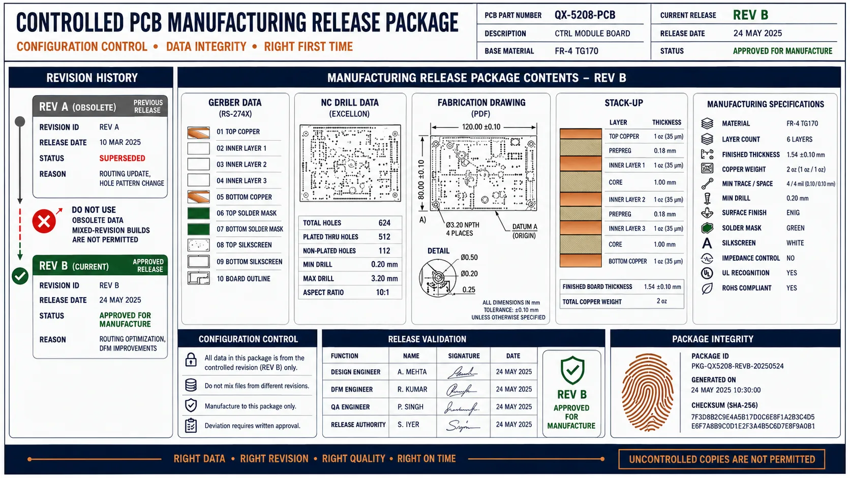
Imagine the supplier receives:
Gerbers from Revision C
drill files from Revision B
fabrication drawing from Revision C
stack-up from an earlier version
Every file may individually appear valid.
Together, they can define the wrong PCB.
A controlled package should therefore have:
part number
revision
release date
controlled file set
change description where appropriate
30. Units, Coordinates, Origin and Scaling
Manufacturing files contain geometric information.
Therefore, verify:
units
coordinate system
origin
scaling
format
precision
An incorrect scaling or coordinate interpretation can produce a board where every feature is geometrically wrong even though the file itself appears technically valid.
This is one reason visual CAM inspection is so important.
31. Overlay the Manufacturing Layers
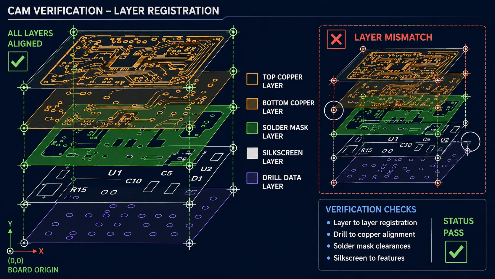
A practical validation method is to overlay:
Top Copper
↓
Bottom Copper
↓
Solder Mask
↓
Silkscreen
↓
Drill Data
The important question is:
Do all manufacturing layers register correctly around the same board geometry?
This can expose:
origin problems
scaling problems
layer offsets
incorrect export settings
drill misalignment
mask-registration errors.
32. Always Open the Final Files in a Gerber/CAM Viewer
This is one of the most important practical rules in both source articles.
Never assume that:
“The CAD software exported successfully, therefore the manufacturing package is correct.”
Open the actual exported package in an appropriate Gerber/CAM viewer.
Review:
Top View
pads
copper
outline
silkscreen
Bottom View
copper
solder mask
silkscreen
bottom-side features
Multilayer View
internal routing
planes
vias
layer order
Drill Overlay
vias
mounting holes
through-holes
slots
The objective is to validate the manufacturing output, not merely the source CAD design.
33. Common Manufacturing-Data and Gerber Errors
a. Missing Layer
A copper or mask layer is absent.
b. Wrong Layer Assignment
An internal copper layer is exported under the wrong identity.
c. Incorrect Board Outline
The outline does not represent the intended finished PCB.
d. Drill Mismatch
Drill locations or sizes do not correspond to pads.
e. Silkscreen Overlap
Reference designators or markings overlap pads or board edges.
f. Wrong Polarity Marking
A marking does not represent the intended component orientation.
g. Missing Cut-Out
A required mechanical opening is absent.
h. Incorrect Mask Opening
A required pad is covered or an unintended region is exposed.
i. Stale Revision
Gerbers were generated before the latest PCB revision.
j. Ambiguous Layer Naming
The manufacturer cannot immediately determine what a file represents.
These are exactly the kinds of problems a structured manufacturing review should catch before fabrication.
34. Gerber Validation Is More Than Visual Inspection
A robust release process can be:
CAD Design Review
↓
Manufacturing Output Generation
↓
Gerber/CAM Visual Inspection
↓
Layer Comparison
↓
Drill Verification
↓
Manufacturing Specification Review
↓
DFM Review
↓
Final Controlled Release
This creates multiple opportunities to identify discrepancies before material is committed.
35. Don't Send Gerbers Without Supporting Specifications
Gerbers communicate geometry.
They may not fully communicate:
stack-up
material
finished thickness
copper thickness
surface finish
impedance
special fabrication requirements
dimensional requirements
inspection requirements
revision
Therefore:
Gerbers + Drill Data + Supporting Specifications = a much more complete manufacturing definition.
36. PCB Fabrication Package vs Complete PCBA Package
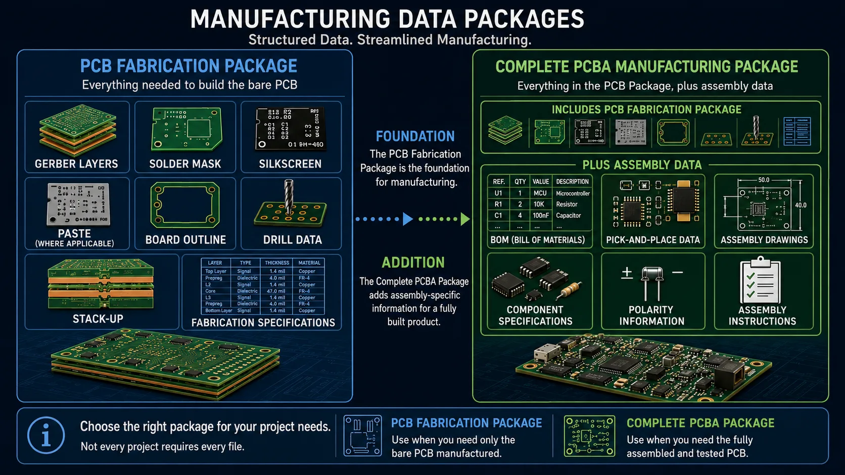
PCB Fabrication Package
May include:
Gerber/manufacturing layers
solder mask
silkscreen
paste where applicable
board outline
drill data
stack-up
fabrication specifications
PCBA Manufacturing Package
May additionally require:
BOM
pick-and-place / centroid data
assembly drawings
component specifications
polarity information
stencil data
assembly instructions
special process requirements
Therefore:
A PCB fabrication package and a complete PCBA manufacturing package should not be treated as identical.
For turnkey PCBA, fabrication, component sourcing and assembly data ultimately need to be coordinated.
37. Advanced PCB Technologies Need More Manufacturing Definition
A simple Gerber export may not be sufficient for complex boards.
Additional consideration may be required for:
HDI
microvias
blind vias
buried vias
sequential lamination
laser-drilled structures
fine-pitch BGA
controlled impedance
heavy copper
metal-core boards
RF/microwave PCBs
rigid-flex
high-layer-count boards
embedded components
Such designs may require explicit information about:
microvia construction
sequential build-up
via filling
laser drilling
registration
dielectric thickness
impedance
material system
For these projects, the manufacturing package should be reviewed with the intended fabrication partner before release.
38. Preparing Manufacturing Files for International PCB Sourcing
When PCB fabrication is sourced internationally, documentation quality becomes even more important.
The supplier may operate in a different:
country
manufacturing environment
CAM workflow
engineering terminology
time zone
quality system
Clear documentation reduces dependence on verbal clarification.
This becomes particularly important when comparing several suppliers.
If Supplier A interprets one requirement differently from Supplier B, their quotations may appear comparable while actually representing different PCB constructions.
That creates a dangerous situation:
Price comparison without technical equivalence.
39. The Manufacturing Package Should Support the RFQ
A good manufacturing package should allow a supplier to quote the same technical product you expect them to manufacture.
For an RFQ, the supplier should be able to establish:
board construction
quantity
layer count
material
thickness
copper
surface finish
special processes
testing
quality requirements
lead-time implications
Therefore, the manufacturing package is not merely a production document.
It is also a commercially important document.
Better-defined requirements generally produce more meaningful supplier comparisons.
40. What Procurement Teams Should Check Before an RFQ
Procurement does not necessarily need to inspect every Gerber coordinate.
But it should confirm that engineering has released a complete package.
Procurement Gate
☐ Correct PCB part number☐ Correct revision☐ Correct quantity☐ Complete fabrication data☐ Drill data included☐ Fabrication drawing included☐ Stack-up defined☐ Material defined☐ Copper defined☐ Finished thickness defined☐ Surface finish defined☐ Special requirements identified☐ Testing requirements defined☐ Quality/acceptance requirements defined
This reduces the risk of receiving quotations based on incomplete assumptions.
41. The Complete Engineering Release Checklist
Before sending the final package to the fabricator:
Design Data
☐ Final design revision released☐ Design-rule checks completed☐ No unresolved design violations☐ Correct layer count
Fabrication Data
☐ Gerber/approved manufacturing data exported☐ NC drill files exported☐ Board outline verified☐ Slots and cut-outs verified☐ Solder mask verified☐ Silkscreen verified
Construction
☐ Stack-up defined☐ Material defined☐ Finished thickness defined☐ Copper thickness defined☐ Surface finish defined
Electrical
☐ Controlled impedance defined where applicable☐ Electrical-test requirements defined☐ Special electrical requirements documented
Mechanical
☐ Dimensions verified☐ Hole requirements verified☐ Edge features verified☐ Mounting features verified
Quality
☐ Applicable IPC/customer requirements defined☐ Product classification established where applicable☐ Acceptance criteria identified
Configuration
☐ Part number correct☐ Revision correct☐ All files belong to the same release☐ Manufacturing package reviewed in CAM viewer
42. The 10-Minute Pre-Release Sanity Check
Before uploading the package to a supplier portal or sending it by email, stop and ask:
Can I identify every PCB layer?
Can I identify every hole type?
Can I identify the exact board outline?
Is the stack-up unambiguous?
Is finished thickness defined?
Is copper thickness defined?
Is surface finish defined?
Are controlled-impedance requirements defined where needed?
Is the applicable quality/acceptance requirement clear?
Can I prove that every file belongs to the same revision?
If the answer to any of these is no, the package deserves another engineering review before release.
43. What Should the Fabricator Do With Your Files?
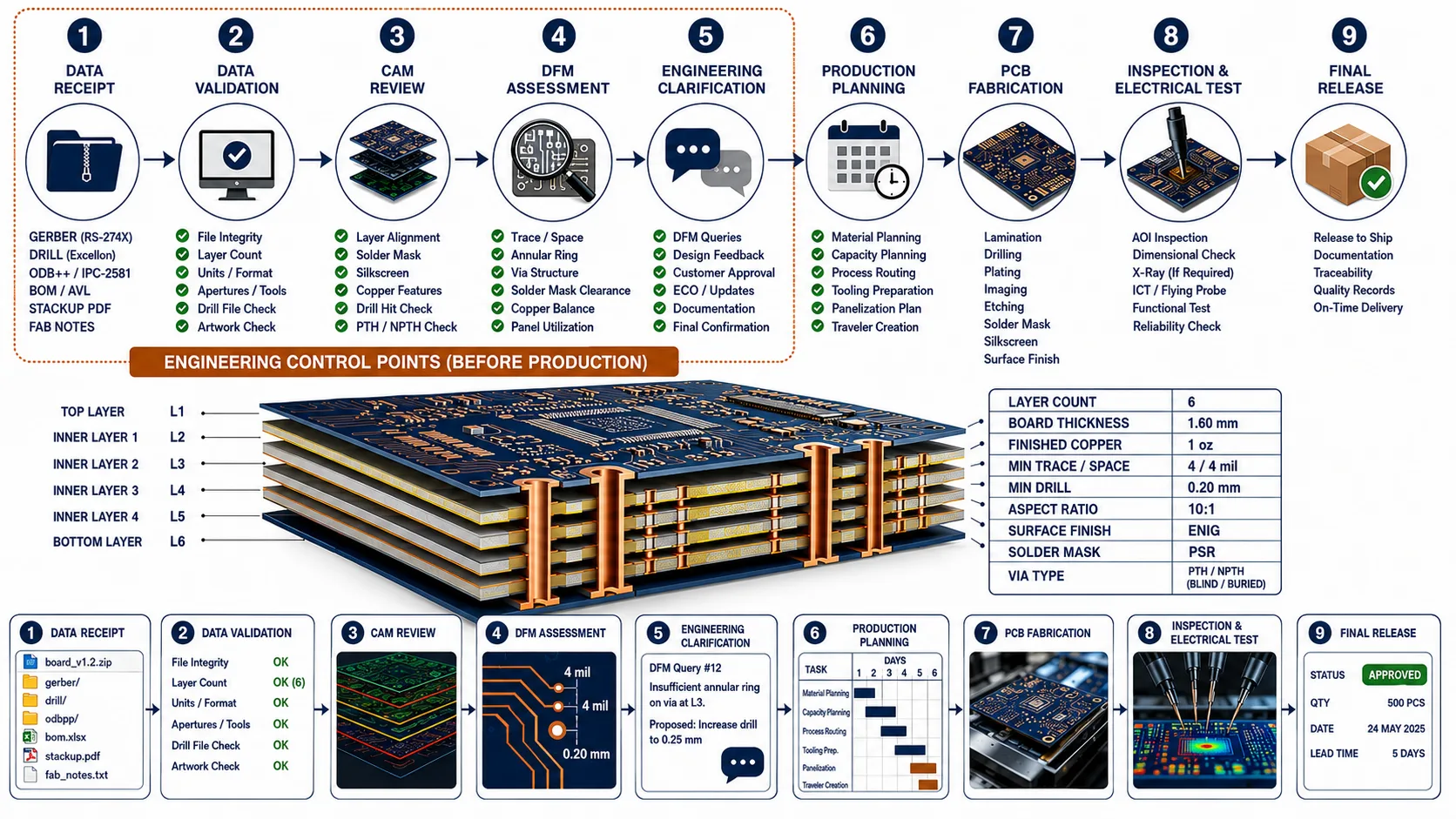
A technically mature supplier workflow should not simply be:
Receive files → Manufacture
A better workflow is:
Receive Manufacturing Package
↓
Data Validation
↓
CAM Review
↓
DFM Review
↓
Manufacturing Clarification
↓
Production Planning
↓
Fabrication
↓
Inspection & Testing
↓
Final Release
The supplier's engineering team should identify ambiguities before production rather than silently making assumptions.
44. Why This Matters to the Supplier
A complete manufacturing package does not only protect the customer.
It also helps the fabricator.
Clear documentation can reduce:
engineering clarification cycles
CAM rework
quotation ambiguity
manufacturing assumptions
production delays
revision confusion
yield risk
Therefore, detailed questions from an experienced fabricator should not automatically be viewed as friction.
In many cases, they indicate that the supplier is actually examining the manufacturing requirements.
45. From Manufacturing Files to Manufacturing Confidence
The ultimate objective is not to create a large ZIP file.
It is to create manufacturing confidence.
The supplier should know:
WHAT
What PCB is being built?
HOW
What construction and manufacturing requirements apply?
WHERE
Where are the copper features, holes, outline and mechanical features?
HOW WELL
What tolerances, quality requirements and acceptance criteria apply?
WHICH VERSION
Which revision is the approved production release?
That is the difference between a collection of exported files and a controlled manufacturing release.
46. The Complete Manufacturing Release Workflow
A robust engineering workflow can therefore be:
Freeze Design Revision
↓
Confirm Manufacturing Requirements
stack-up
material
copper
thickness
finish
impedance
special requirements
↓
Generate Gerber / Approved Manufacturing Data
↓
Generate NC Drill Data
↓
Prepare Fabrication Drawing and Specifications
↓
Open the Exported Package
↓
Overlay and Inspect
copper
mask
silkscreen
outline
drill
↓
Compare Against Original PCB Design
↓
Perform DFM / Manufacturing Review
↓
Package Supporting Documentation
↓
Release Controlled Manufacturing Package
↓
Supplier Engineering Review
↓
Production Planning
↓
Fabrication
↓
Inspection & Electrical Test
↓
Final Release
This brings together the strongest workflow elements from both original articles.
47. The Most Important Rule
There is one principle worth remembering above everything else:
Validate the files you actually send to the manufacturer—not merely the design that exists inside your CAD software.
The correct sequence is:
Design
↓
Export
↓
Open the exported files
↓
Inspect
↓
Compare against design
↓
Correct if necessary
↓
Release final package
The files that matter to the manufacturer are the files that were actually released—not the version that happens to be open in the designer's CAD environment.
48. Final Takeaway
Preparing PCB manufacturing files correctly is not simply a matter of clicking “Export.”
A production-ready manufacturing package should be:
complete
correctly layered
correctly identified
correctly aligned
supported by appropriate drill data
supported by stack-up and fabrication specifications
revision-controlled
CAM/DFM reviewed
visually inspected
validated against the original PCB design
The most important questions are:
Is every required layer present?
Are the layers correctly identified and aligned?
Does the board outline represent the actual finished PCB?
Does the drill data match the copper artwork?
Are plated and non-plated holes clearly defined?
Is the physical stack-up unambiguous?
Are material, copper, thickness and surface finish defined?
Are controlled-impedance requirements properly specified?
Are quality and acceptance requirements clear?
Does every file belong to the same approved revision?
Can the supplier quote and manufacture the same technical product that the engineering team intended?
If the answer to all of these is yes, the manufacturing handoff becomes significantly more controlled.
49. QUADRIONIX Perspective
The manufacturing package is the foundation of the engineering-to-production handoff.
A structured workflow can begin with:
Customer PCB Manufacturing Data
↓
Data & DFM Review
↓
Manufacturing Requirements Confirmation
↓
Fabrication Planning
↓
PCB Production
↓
Inspection & Testing
↓
Final Release
For PCBA projects, this can extend through:
PCB Fabrication → Component Sourcing → SMT/THT Assembly → Inspection → Testing → Production Readiness
The objective is straightforward:
Reduce ambiguity between the customer's engineering intent and the physical product being manufactured.
This becomes particularly important for international sourcing programs, where clear manufacturing data provides a common technical reference between customer, supplier and production teams.
Frequently Asked Questions
Ready to manufacture your electronics project?
Upload your Gerber files & BOM for automated DFM review, engineering feedback, and guaranteed delivery timelines.