How to Plan Test Points for PCB Assembly
A practical guide to designing PCB test points for ICT, flying probe and functional testing—before manufacturing begins

PCB test point design for ICT flying probe and functional testing
Testing a PCB after assembly sounds straightforward:
Connect the test equipment.
Probe the board.
Measure the required signals.
Confirm that it works.
But the reality is that testing begins much earlier than the test station.
It begins during PCB design.
Where test points are placed, how accessible they are, how much spacing exists between them, which signals are exposed, and whether the board can physically interface with the test equipment can all influence the eventual manufacturing test strategy.
A PCB that was designed without testability in mind may require:
This is why Design for Testability (DFT) should be considered alongside Design for Manufacturing (DFM).
The objective is simple:
Make the PCB easy to manufacture, easy to inspect and easy to test.
1. What Is a PCB Test Point?
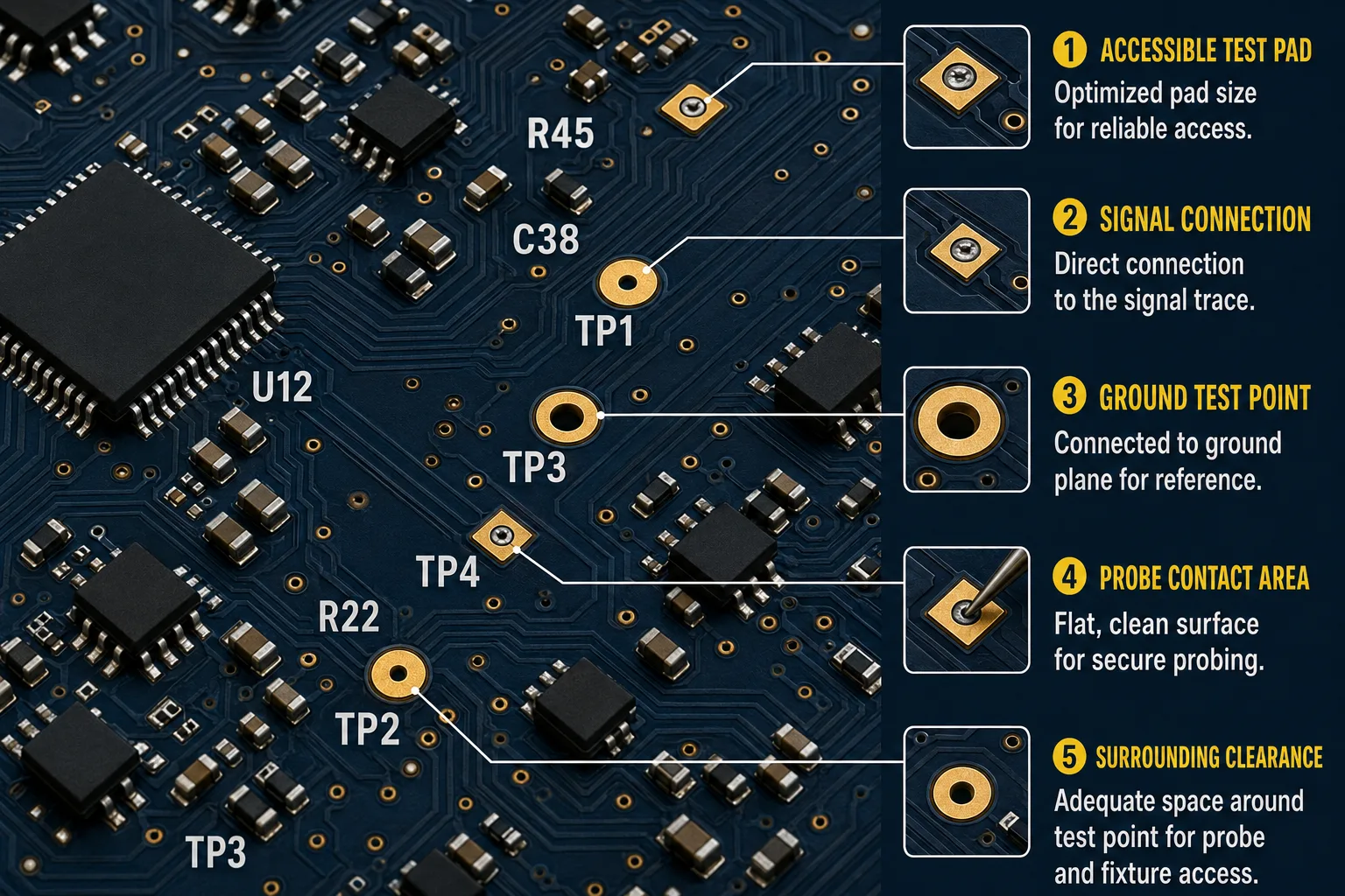
A properly designed test point provides reliable physical access to a defined electrical node.
A PCB test point is an accessible electrical connection designed specifically to allow a probe or test instrument to contact a particular electrical node.
A test point may provide access to:
The test point provides a controlled interface between the PCB and the test equipment.
Instead of trying to contact an individual component lead or tiny IC pin, the manufacturing test system can access a deliberately designed pad.
2. Why Test Points Matter
Test points can support several manufacturing and engineering activities.
Production testing
ICT and other electrical test systems can use them to verify circuit behavior.
Debugging
Engineers can connect probes or instruments during development.
NPI validation
Test points can help manufacturing teams diagnose problems during early production.
Functional testing
Selected signals can be accessed during system-level test procedures.
Field diagnostics
For some products, accessible test points can also support engineering diagnostics and troubleshooting.
Therefore, test points are not merely manufacturing features.
They can become part of the PCB's broader diagnostic architecture.
3. Test Points and Design for Testability
Design for Testability—or DFT—is the practice of designing a product so that it can be tested efficiently and reliably.
DFT considerations can include:
The earlier these considerations are introduced, the easier it is to integrate them into the PCB layout.
4. Test Points Should Be Planned Before Layout Is Finished
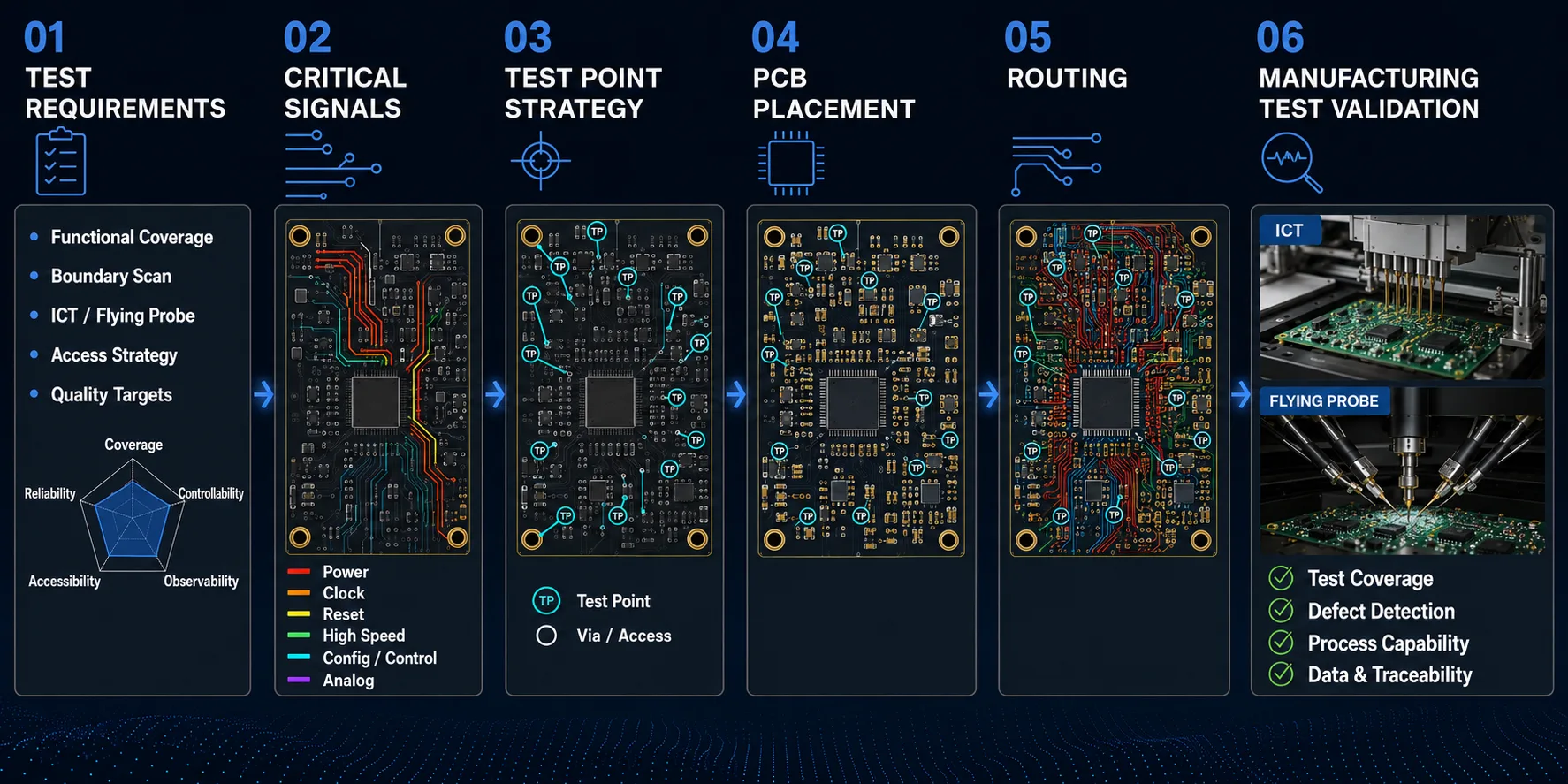
Testability is most effective when test-point planning begins before PCB layout is finalized.
One common mistake is treating test points as an afterthought.
The PCB is routed.
The board is nearly complete.
Then someone asks:
"Where are we going to probe this circuit?"
At that point, adding test points may create conflicts with:
A better approach is:
Test strategy → Signal selection → Test-point planning → PCB layout
rather than:
PCB layout → Test-point problem → Late redesign
5. Which Signals Should Have Test Points?
You do not necessarily need a test point for every electrical node.
The goal is to provide access to signals that are important for:
Typical candidates can include:
Power rails
Examples:
Ground
A reliable ground reference is often important for measurements.
Communication interfaces
Depending on the design:
Critical analog signals
Where measurement is useful for:
Important digital signals
Especially where they are needed to verify a subsystem.
Programming/debug interfaces
Where relevant to the production process.
6. Critical Signals vs Every Signal
More test points do not automatically mean better testability.
Excessive test points can consume:
The better question is:
Which nodes provide the greatest diagnostic and manufacturing value?
A well-designed test strategy identifies important nets and makes them accessible.
7. Ground Test Points
Ground deserves special consideration.
A stable ground reference may be required for:
Where appropriate, dedicated ground test points can make probing easier and more reliable.
The exact arrangement should be compatible with the selected testing method and equipment.
8. Test Point Accessibility
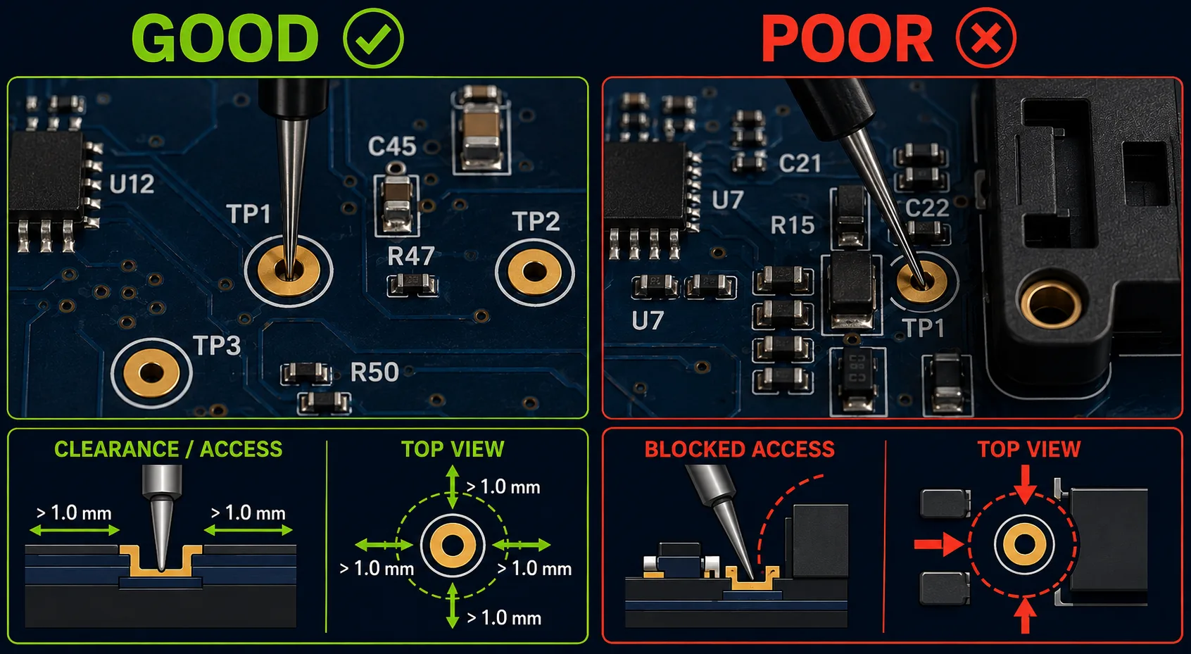
A test point must be electrically connected and physically accessible to the intended test equipment.
A test point is useful only if the test equipment can actually reach it.
This sounds obvious.
But PCB layouts can create accessibility problems.
For example, a test pad may be:
Therefore:
Electrical connectivity is only half the requirement. Physical accessibility matters equally.
9. Test Point Size
Test-point dimensions should be selected based on:
A test point should be large enough to provide reliable probe contact while fitting within the available PCB area.
There is no universal size that is correct for every design.
The test equipment and manufacturing partner should be considered when establishing the design rules.
10. Test Point Spacing
Spacing is particularly important for automated probing.
If test points are too close together, probes may have difficulty making reliable individual contact.
Insufficient spacing can create risks such as:
Spacing requirements depend on:
Therefore, test-point spacing should be established against the actual test method rather than using an arbitrary value.
11. One-Side Test Points Can Simplify Testing
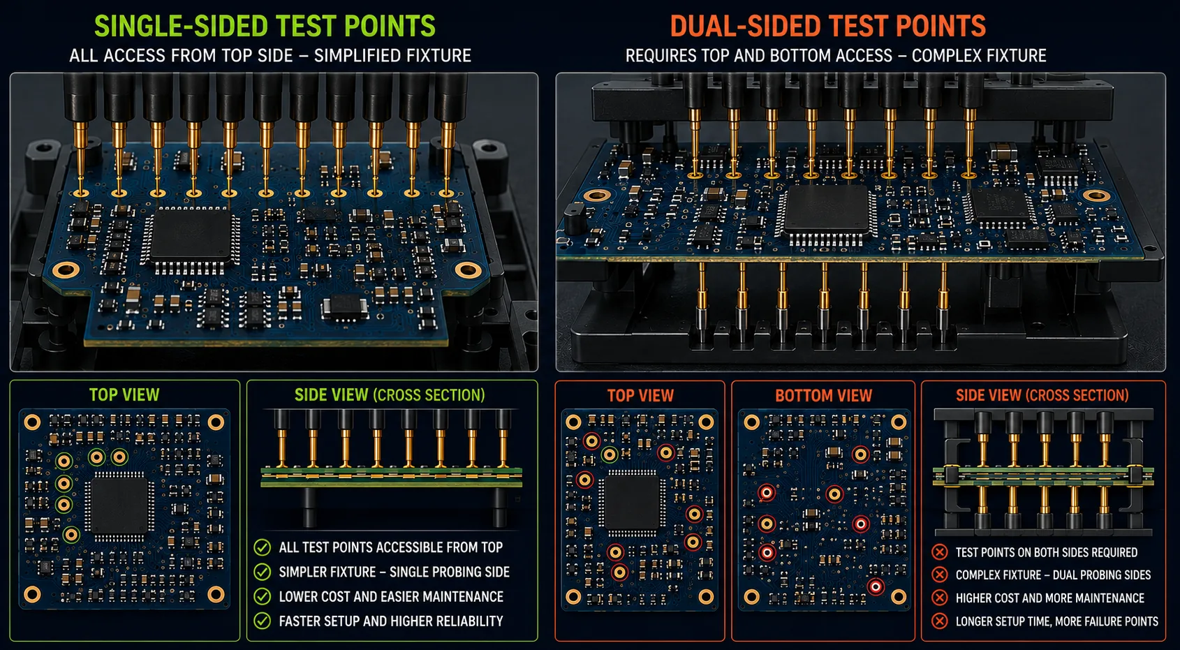
Single-sided test access can simplify fixture design, while complex boards may require dual-sided access.
Where practical, placing test points on a common PCB side can simplify fixture design.
A one-sided test strategy may reduce:
However, this is not always possible.
Dense PCB layouts, mechanical constraints or signal accessibility requirements may require test points on both sides.
The correct decision depends on the product.
12. Test Points and SMT Assembly
Test points must coexist with the assembly process.
Design teams should consider:
The test point should not create an unintended manufacturing problem.
For example, an exposed copper pad in the wrong location could interfere with soldering or create an unintended solder connection.
13. Test Points and Solder Mask
Whether a test pad is covered or exposed depends on the intended testing method.
A probe generally needs access to the conductive surface.
Therefore, test-point definitions should clearly communicate the intended manufacturing requirement.
This should be captured in the PCB design data and manufacturing documentation.
The exact implementation should be reviewed with the PCB fabricator and assembly/test provider.
14. Test Points Near Fine-Pitch Components
Fine-pitch components can make test-point planning more challenging.
The designer may need to balance:
Electrical access
against:
Available PCB area
against:
Probe clearance
against:
Routing density
A good strategy is to identify critical signals early and reserve suitable areas for test access.
15. Test Points for BGA-Based Designs
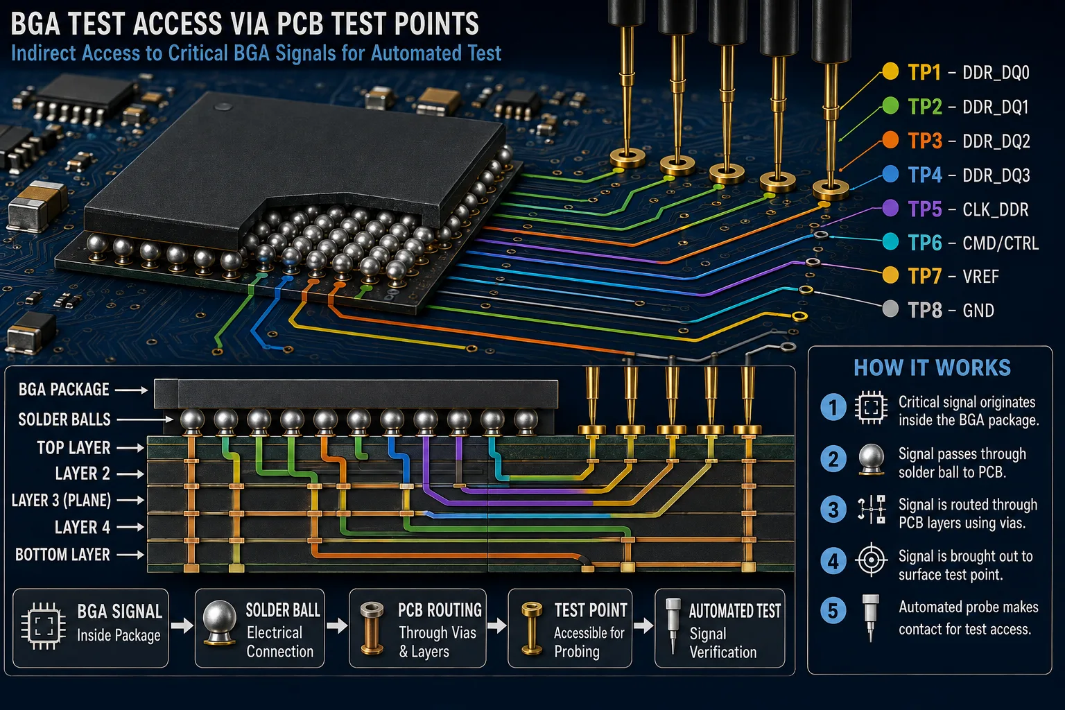
Critical signals connected to hidden BGA connections can be routed to accessible test nodes where appropriate.
BGA packages introduce additional challenges because many signals terminate beneath the package.
Direct probing of BGA solder joints is generally not practical.
Therefore, designers should consider bringing important BGA-connected signals to accessible nodes elsewhere in the circuit where appropriate.
This could involve:
The objective is not necessarily to expose every BGA connection.
It is to ensure that important signals can still be verified.
16. Test Points for ICT
ICT typically relies on a defined set of accessible electrical nodes.
The test strategy may require access to:
The PCB design should therefore be reviewed against the intended ICT requirements before manufacturing.
ICT planning should also consider fixture mechanics.
17. Test Points for Flying Probe
Flying probe systems provide greater flexibility because probes can move to different locations.
However, accessibility and spacing remain important.
The system still needs:
Therefore:
Flying probe reduces fixture dependency, but it does not eliminate PCB testability requirements.
18. Test Points for Functional Testing
Functional testing may not require the same test-point architecture as ICT.
A functional test could interface through:
The test strategy should therefore be defined based on what the functional test needs to stimulate and measure.
19. Test Points and Programming
Many modern PCB assemblies require programming during production.
For example:
Production programming may require access to:
These interfaces should be considered early in the design.
20. Test Points Can Support Debugging During NPI
Test points are especially valuable during NPI.
Imagine a prototype that fails functional testing.
Without accessible measurement points, the engineer may have to:
With appropriate test points, the engineer can quickly measure:
This can significantly simplify troubleshooting.
21. Test Points and Design Revisions
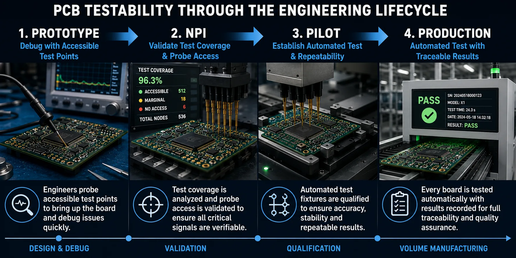
Test-point planning should evolve with the product from engineering prototype through production.
PCB designs often change during NPI.
If the test architecture is tightly integrated into the design, engineering changes can affect:
Therefore, whenever the PCB revision changes, the test strategy should also be reviewed.
A new PCB revision should not automatically be assumed to remain fully test-compatible.
22. Test Points and PCB Size
Every test point occupies physical space.
On a large PCB this may be relatively easy to accommodate.
On a compact board, test points compete with:
This makes early planning particularly important for compact electronics.
23. Don't Put Test Points Where Probes Cannot Reach
A technically connected pad may still be practically useless.
Before finalizing the layout, review:
Top-side access
Can the probe reach it?
Bottom-side access
Is bottom-side probing possible?
Component clearance
Will components obstruct the probe?
Mechanical clearance
Will the enclosure or fixture interfere?
Probe angle
Can the intended probe approach the pad correctly?
This physical review can prevent expensive fixture problems later.
24. Test Point Naming and Documentation
Test points should be clearly identified in the engineering documentation.
Examples:
The exact naming convention is less important than consistency.
Documentation should ideally allow:
Designer → Manufacturer → Test Engineer
to understand what each test point represents.
25. Test Point Data Should Be Part of the Manufacturing Package
Depending on the manufacturing/test process, useful test documentation may include:
This information can help the manufacturing partner develop or validate the test process.
26. Common PCB Test-Point Mistakes
Mistake 1 — Adding test points at the end
This can create layout conflicts.
Mistake 2 — Providing too few test points
Important circuits may become difficult to diagnose.
Mistake 3 — Providing too many
Excessive test points consume valuable PCB area.
Mistake 4 — Poor spacing
Probes may interfere with one another.
Mistake 5 — Poor physical access
Components or mechanical features may block the probe.
Mistake 6 — No ground access
Measurements can become unnecessarily difficult.
Mistake 7 — Ignoring BGA signals
Important hidden connections may lack accessible test nodes.
Mistake 8 — Not considering production volume
The most appropriate test architecture for prototypes may differ from high-volume production.
Mistake 9 — Not reviewing PCB revisions
A design change can invalidate test access.
Mistake 10 — Treating testing as someone else's problem
DFT is a cross-functional design responsibility.
27. Test Points and Manufacturing Cost
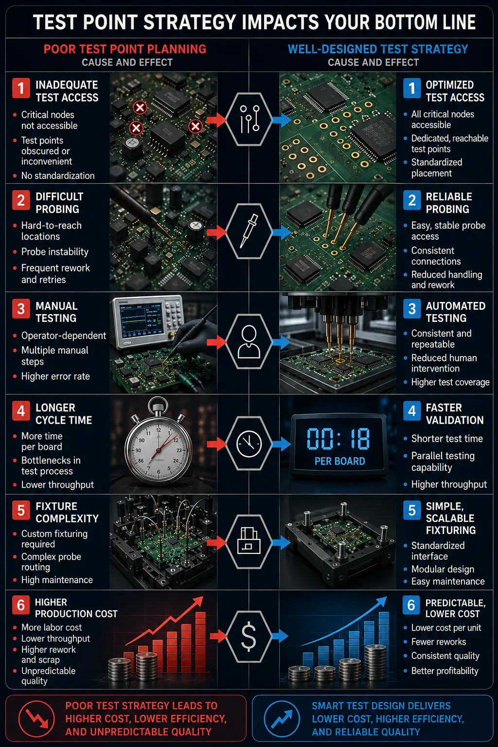
Good testability can reduce avoidable manufacturing complexity and testing cost.
Test points themselves are inexpensive PCB features.
But poor testability can create larger costs.
For example:
Poor test access
→ custom engineering workaround
→ more manual testing
→ longer cycle time
→ additional fixture complexity
→ higher production cost
Therefore:
Testability should be evaluated as part of total manufacturing economics.
28. Test Points and High-Volume Production
At high production volumes, test efficiency becomes increasingly important.
A few seconds saved per PCB can become significant when multiplied across:
10,000
100,000
or
1,000,000 assemblies.
This makes:
important manufacturing considerations.
29. Test Points and Low-Volume Production
Low-volume production has a different economic profile.
A dedicated ICT fixture may not always be justified.
Flying probe or manual/semiautomated testing may provide greater flexibility.
Again, the correct strategy depends on:
30. A Practical Test-Point Planning Workflow
A useful workflow is:
Step 1 — Define the test objectives
What must be verified?
Step 2 — Identify critical signals
Which nets are important for manufacturing and debugging?
Step 3 — Select the test method
ICT?
Flying probe?
Functional test?
Combination?
Step 4 — Define test-point requirements
Pad type, accessibility, spacing and location.
Step 5 — Place test points
Reserve suitable PCB areas.
Step 6 — Route the board
Ensure the test-point strategy remains intact.
Step 7 — Review mechanical accessibility
Check probes, fixtures and enclosure constraints.
Step 8 — Validate test coverage
Confirm that the intended test can actually access required signals.
Step 9 — Release manufacturing documentation
Provide the required test data.
Step 10 — Validate during NPI
Confirm that the real assembled PCB can be tested reliably.
31. PCB Test Point Checklist
Before releasing a PCB for manufacturing:
Electrical
Physical
Manufacturing
NPI
32. Should Every PCB Have Test Points?
Not necessarily.
The appropriate approach depends on:
For a simple low-volume product, extensive test-point architecture may not provide enough value.
For a complex production product, testability can be extremely important.
The key is to make the decision deliberately.
33. The Most Important Principle
The most important test-point principle is:
Design access before you need access.
If a product fails during NPI, manufacturing engineers should be able to investigate it.
If production requires electrical verification, the board should interface efficiently with the test equipment.
If a field-return investigation occurs, engineering should have useful diagnostic access where appropriate.
Good test-point planning makes all three situations easier.
34. FINAL TAKEAWAY
PCB test points may be small features on a circuit board, but they can have a significant influence on manufacturing, testing and debugging.
Good test-point planning considers:
What needs to be tested?
How will it be tested?
Where will the probe contact the PCB?
Can the probe physically reach the point?
Is there enough spacing?
Does the point remain accessible after assembly?
Will the test strategy scale from prototype to production?
The best approach is to integrate testability into PCB design rather than adding test points after routing is complete.
A well-designed PCB should support the full manufacturing lifecycle:
Design
→ Fabrication
→ Assembly
→ Inspection
→ Electrical Testing
→ Functional Validation
→ Production
35. QUADRIONIX PERSPECTIVE
At QUADRIONIX, testability is always considered as part of the PCB manufacturing strategy—not as an isolated activity at the end of assembly.
A production-ready design should bring together:
→ DFM
→ DFT
→ Assembly
→ Inspection
→ Electrical Test
→ Functional Validation
→ Traceability
For international customers, early test-point planning can help reduce avoidable fixture development, manual probing and production troubleshooting.
The objective is not simply to add more test pads.
It is to create the right test access for the right manufacturing and validation strategy.
If you are Planning a PCB/PCBA production program, our engineering and manufacturing team can review testability considerations before production and help align the PCB design with the intended assembly and testing process.
Design for manufacturing. Design for test. Build with confidence.
Frequently Asked Questions
Ready to manufacture your electronics project?
Upload your Gerber files & BOM for automated DFM review, engineering feedback, and guaranteed delivery timelines.