How to Choose the Right PCB Stack-Up and Surface Finish
A Practical Engineering Guide to Layer Configuration, Impedance Control, Reliability, Manufacturability and Surface-Finish Selection
Introduction
Two PCB design decisions can have a disproportionate effect on manufacturing performance:
How the PCB is constructed internally
and
How its exposed copper surfaces are finished.
The first is primarily a stack-up decision.
The second is a surface-finish decision.
Neither should be selected simply because it is commonly used or because a previous board used the same specification.
A PCB stack-up affects:
Surface finish affects:
The correct selection therefore begins with the electrical, mechanical, environmental and manufacturing requirements of the product.
1. Stack-Up and Surface Finish Are Different Decisions
This distinction is important.
PCB stack-up
Defines the internal construction of the board:
Surface finish
Defines the treatment applied to exposed copper areas intended for soldering or electrical contact.
Examples include:
Therefore:
Stack-up determines how the PCB is constructed. Surface finish determines how exposed copper is protected and prepared for use.
They should be specified separately.
2. Start With the Electrical Requirements
Do not begin stack-up selection by saying:
“I need an 8-layer board.”
Instead, begin with the electrical architecture.
Ask:
The stack-up should be derived from these requirements.
3. Layer Count Is Not the Same as Signal Integrity
More layers do not automatically mean better signal integrity.
A well-designed six-layer stack-up can outperform a poorly constructed eight-layer stack-up.
For high-speed design, the critical questions include:
The relationship between copper layers and dielectric geometry is often more important than simply counting layers.
4. Understand the Basic PCB Stack-Up
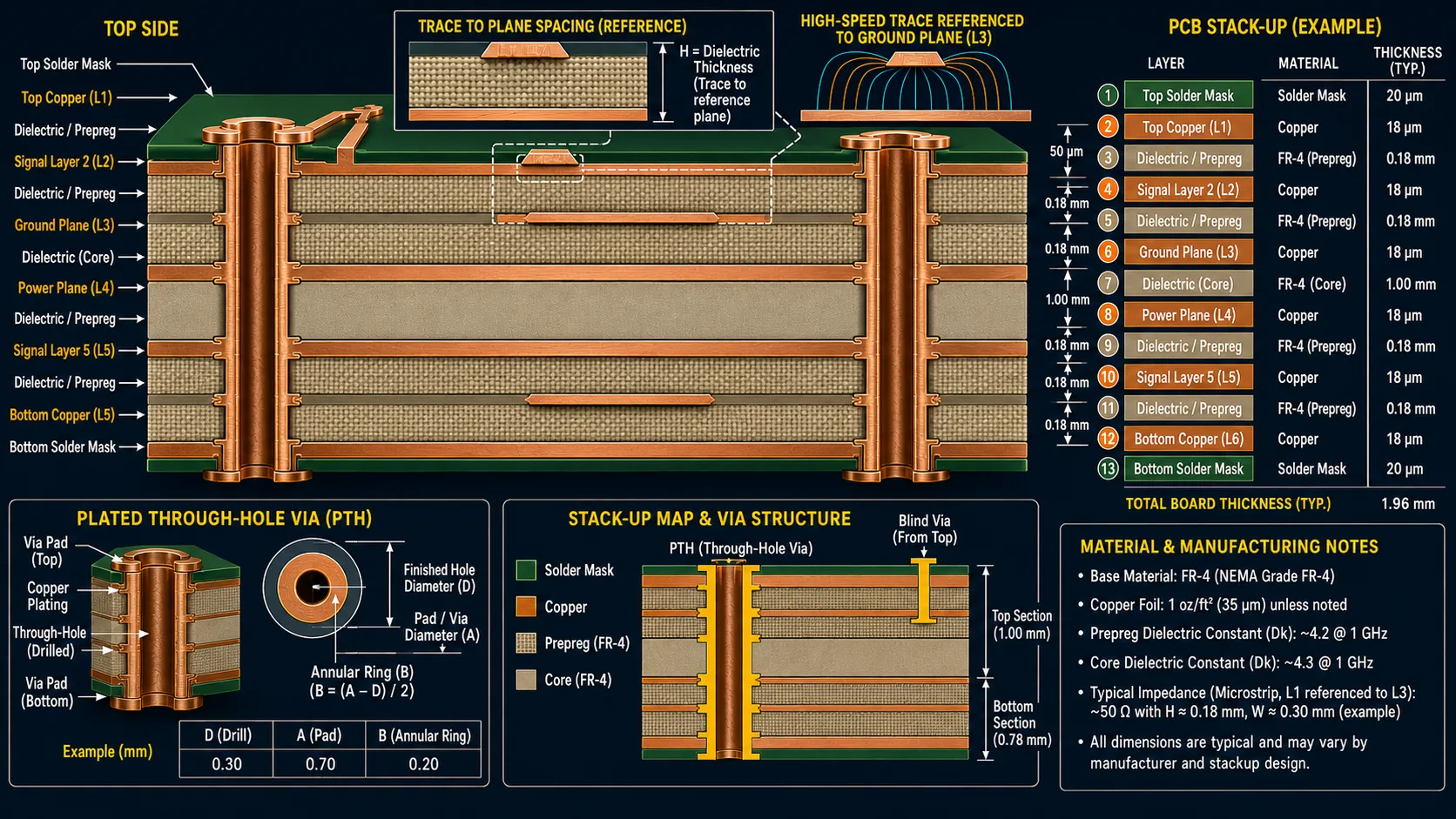
PCB stack-up defines the relationship between signal layers, reference planes, dielectric structures and copper thickness.
A simplified multilayer PCB construction may look like:
Top solder mask
↓
Top copper
↓
Prepreg / dielectric
↓
Internal copper plane
↓
Core
↓
Internal copper plane
↓
Prepreg / dielectric
↓
Bottom copper
↓
Bottom solder mask
Actual constructions can be substantially more complex.
A six-layer board, for example, may contain multiple signal and plane layers separated by different dielectric structures.
5. Why Reference Planes Matter
A high-speed signal does not exist electrically by itself.
Its return current must follow an appropriate path.
For many PCB structures, the return current is concentrated around the signal trace and its reference plane.
A continuous ground plane can therefore provide:
If a high-speed trace crosses a discontinuity in its reference plane, its return path can be disrupted.
That can increase:
Therefore, stack-up selection and routing strategy must be considered together.
6. Controlled Impedance Starts With the Stack-Up
Controlled impedance is not achieved simply by specifying:
“50 Ω impedance.”
The manufacturer needs enough information to construct the physical geometry that produces the required impedance.
Important variables include:
For differential pairs, additional variables include:
Therefore:
The PCB stack-up is part of the impedance-control specification.
7. Microstrip vs Stripline
Two common controlled-impedance structures are:
Microstrip
A signal trace is located on an outer layer and referenced primarily to an adjacent internal plane.
Stripline
A signal trace is embedded between reference planes.
A simplified representation:
Microstrip
Signal────────────Dielectric────────────Ground plane
Stripline
Ground plane────────────DielectricSignalDielectric────────────Ground plane
Stripline can provide strong electromagnetic containment and a controlled environment, while microstrip can be useful where component access and routing flexibility are important.
The correct choice depends on the board architecture.
8. Do Not Treat Dielectric Constant as a Single Universal Number
PCB materials are often discussed using dielectric constant, or Dk.
But the effective electrical behavior of a PCB depends on:
For high-speed designs, the designer and fabricator should use the appropriate material data and stack-up construction rather than relying blindly on a generic FR-4 Dk value.
This becomes increasingly important as signal rise times become faster.
9. Glass-Weave Effects Can Matter at High Speed
FR-4 is not electrically homogeneous at microscopic scale.
The dielectric structure contains woven glass reinforcement embedded within resin.
Because the effective dielectric environment can vary depending on whether a trace runs predominantly over glass bundles or resin-rich regions, high-speed signals can experience local propagation variation.
This can become relevant for:
Possible design approaches include:
The importance depends on the interface and edge rate.
10. Copper Thickness Matters Electrically and Thermally
Copper thickness is not just a current-carrying decision.
It also affects:
For power paths, heavier copper may be beneficial.
For dense high-speed routing, however, excessive copper thickness can make fine geometries more difficult.
Therefore:
Copper thickness should be selected from the combined electrical, thermal and manufacturing requirements.
11. When Should You Add More PCB Layers?
Additional layers may be justified by:
But additional layers increase:
The objective is therefore:
The minimum practical layer count that satisfies the electrical, mechanical and manufacturing requirements.
12. A Typical High-Speed Stack-Up Strategy
For a high-speed digital design, a common engineering objective is to place critical signal layers close to continuous reference planes.
For example:
L1 — Signal
L2 — Ground
L3 — Signal
L4 — Power/Ground
L5 — Signal
L6 — Ground
L7 — Signal
L8 — Ground/Power
This is only an example—not a universal prescription.
The actual stack-up should be optimized around:
13. Power Integrity Also Influences Stack-Up
The stack-up influences the physical relationship between power and ground planes.
A close plane-to-plane arrangement can reduce loop inductance and improve high-frequency power-distribution behavior.
Important factors include:
Therefore, stack-up optimization should consider power integrity, not just signal routing.
14. Thermal Requirements Can Change the Stack-Up
Power electronics may require:
For high-current designs, the stack-up may need to accommodate thermal and current-density requirements that would not exist on a low-power digital board.
Examples include:
15. Mechanical Requirements Matter Too
The stack-up also determines overall PCB thickness and mechanical construction.
Consider:
A theoretically ideal electrical stack-up is not useful if it does not fit the mechanical system.
16. Surface Finish: What Is It Actually Doing?
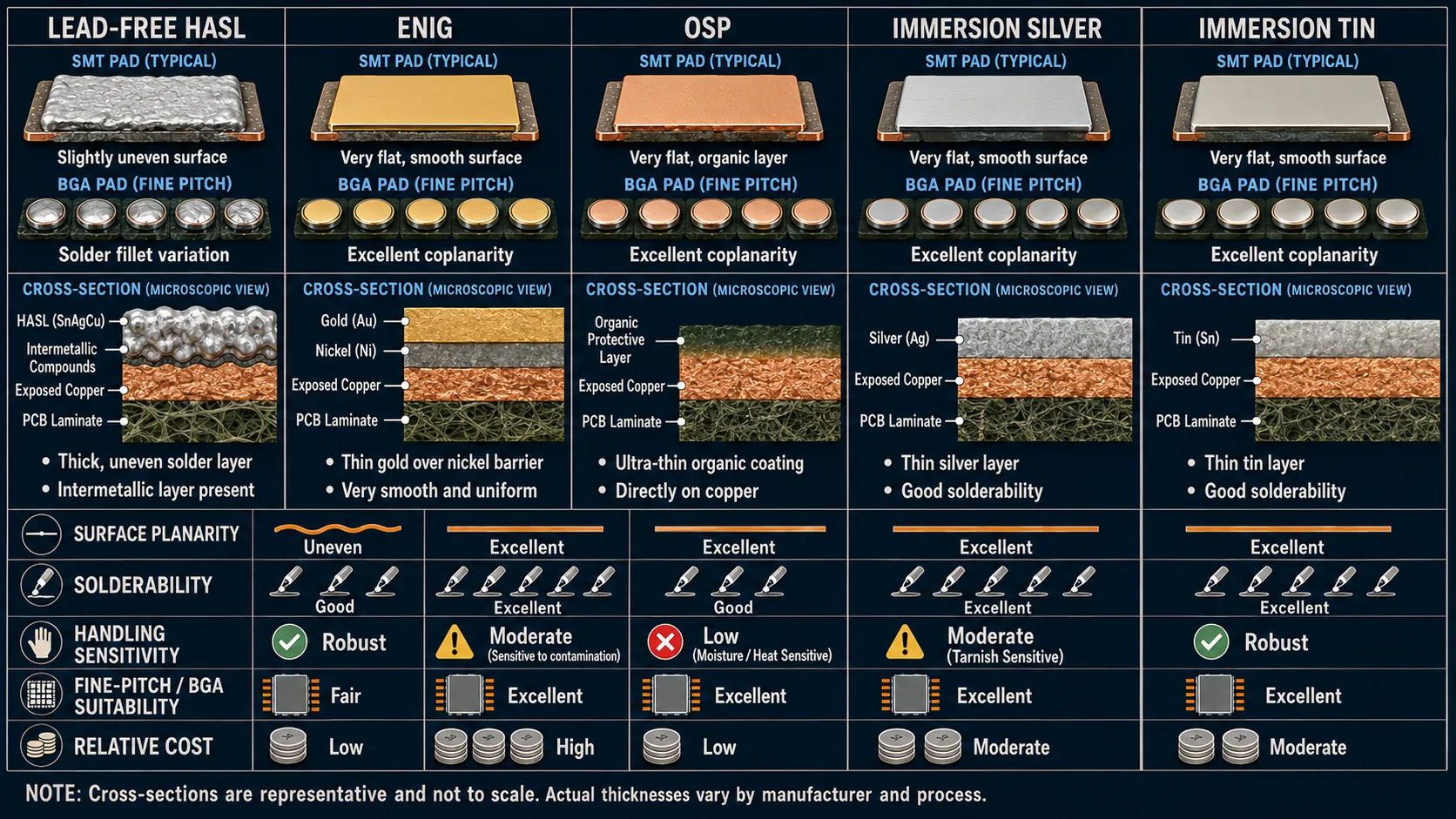
Surface-finish selection should consider solderability, planarity, handling, reliability, application requirements and manufacturing economics.
Surface finish protects exposed copper and provides a suitable surface for:
Bare exposed copper can oxidize and degrade solderability.
The surface finish therefore provides both manufacturing and reliability functions.
But there is no universally best finish.
Selection depends on:
17. HASL
Hot Air Solder Leveling (HASL) uses molten solder to coat exposed copper surfaces, followed by removal of excess solder.
Advantages
Considerations
Traditional HASL can produce a less planar surface than finishes such as ENIG.
This can become important for:
Lead-free HASL is commonly used where lead-free manufacturing is required.
18. ENIG
Electroless Nickel Immersion Gold (ENIG) consists of an electroless nickel layer with a thin immersion-gold layer.
Advantages
Considerations
ENIG is a common choice for boards requiring a flat, consistent surface for modern SMT assembly.
19. OSP
Organic Solderability Preservative (OSP) uses an organic coating to protect exposed copper.
Advantages
Considerations
OSP can be attractive for high-volume SMT applications where the board's storage, handling and assembly conditions are well controlled.
20. Immersion Silver
Immersion silver deposits a thin silver layer over copper.
Advantages
Considerations
21. Immersion Tin
Immersion tin creates a tin surface over the copper.
Advantages
Considerations
It should be selected based on the actual manufacturing and environmental requirements rather than purely on cost.
22. ENIG vs HASL: A Practical Decision
A simplified decision can be:
Consider lead-free HASL when:
Consider ENIG when:
But these are engineering guidelines—not absolute rules.
23. OSP vs ENIG
Both can provide a relatively flat soldering surface.
However, they differ fundamentally.
OSP
Provides an organic protective layer over copper.
ENIG
Provides a metallic nickel/gold surface system.
This difference affects:
Therefore, the correct selection depends on the board's complete lifecycle.
24. Surface Finish for Edge Contacts Is Different
A PCB edge connector is not simply another soldering pad.
Repeated mechanical insertion and removal requires a durable contact surface.
Applications may require:
The finish must therefore be specified according to the mechanical contact requirement, not merely solderability.
25. ENIG Is Not the Same as Hard Gold
This is a common source of confusion.
ENIG
Designed primarily as a solderable PCB surface finish.
Hard gold
Used for durable electrical contacts exposed to mechanical wear.
They are not interchangeable simply because both involve gold.
For an edge connector or repeated-contact application, the required gold-plating construction must be specified appropriately.
26. Gold Thickness Matters
The phrase:
“Gold finish”
is incomplete as an engineering specification.
The relevant requirements may include:
For critical applications, the manufacturer should work from an explicit finish specification rather than a generic color description.
27. Surface Finish and Assembly Process
Surface finish selection should be discussed with the assembly process.
Consider:
A finish that works well in one assembly environment may not necessarily be the optimal choice for another.
28. Rework Requirements Matter
If a product is expected to undergo significant:
then the surface finish should be considered as part of the rework strategy.
This is particularly relevant for:
29. Environmental Conditions Matter
Consider the product's operating environment:
For industrial, automotive, aerospace or outdoor products, surface-finish selection should be evaluated together with the broader reliability requirements.
30. Surface Finish Is Not a Substitute for Good PCB Design
A premium surface finish cannot compensate for:
For example, a BGA assembly problem cannot automatically be solved by changing from one surface finish to another.
The entire manufacturing chain matters:
PCB design
↓
Pad geometry
↓
Stack-up
↓
Fabrication
↓
Surface finish
↓
Stencil
↓
Paste deposition
↓
Placement
↓
Reflow
↓
Inspection
31. Stack-Up and DFM Must Be Developed Together
A theoretically optimal stack-up may create manufacturing challenges.
The fabricator must evaluate:
Therefore, the final stack-up should be reviewed with the manufacturing partner before release.
32. Impedance-Controlled Boards Need Fabricator Involvement
For controlled-impedance designs, provide the fabricator with:
The fabricator can then provide an achievable stack-up based on actual production materials and processes.
This is generally more reliable than designing around a generic stack-up and asking the fabricator to reproduce it exactly.
33. Fabricator-Recommended Stack-Up vs Designer-Defined Stack-Up
There are two common approaches.
Designer-defined
The PCB designer specifies:
Useful when:
Fabricator-engineered
The designer provides:
The fabricator proposes the manufacturable construction.
This can be useful when:
For many commercial designs, collaboration between the two is the strongest approach.
34. Don't Specify Only the Number of Layers
A drawing saying:
“8-layer FR-4 PCB”
does not fully define the manufacturing construction.
You may also need:
The more demanding the board, the more important this becomes.
35. Surface Finish Should Be Explicit in the Fabrication Specification
Instead of:
“Gold PCB”
specify the appropriate finish.
For example:
ENIG surface finish
or an application-specific metallic contact specification.
The fabrication drawing and manufacturing documentation should clearly communicate the required finish.
36. Cost Trade-Offs
There is no single cost hierarchy that applies to every supplier and every production volume.
However, surface-finish cost can be influenced by:
Similarly, stack-up cost can increase with:
Therefore:
Cost optimization should be performed after defining the technical requirements—not before.
37. A Practical Stack-Up Selection Workflow
Use this sequence:
Step 1 — Define interfaces
Identify:
Step 2 — Define impedance
Identify required:
Step 3 — Define routing density
Determine:
Step 4 — Define power architecture
Identify:
Step 5 — Define mechanical constraints
Determine:
Step 6 — Define manufacturing constraints
Evaluate:
Step 7 — Finalize stack-up
Then validate:
38. A Practical Surface-Finish Selection Workflow
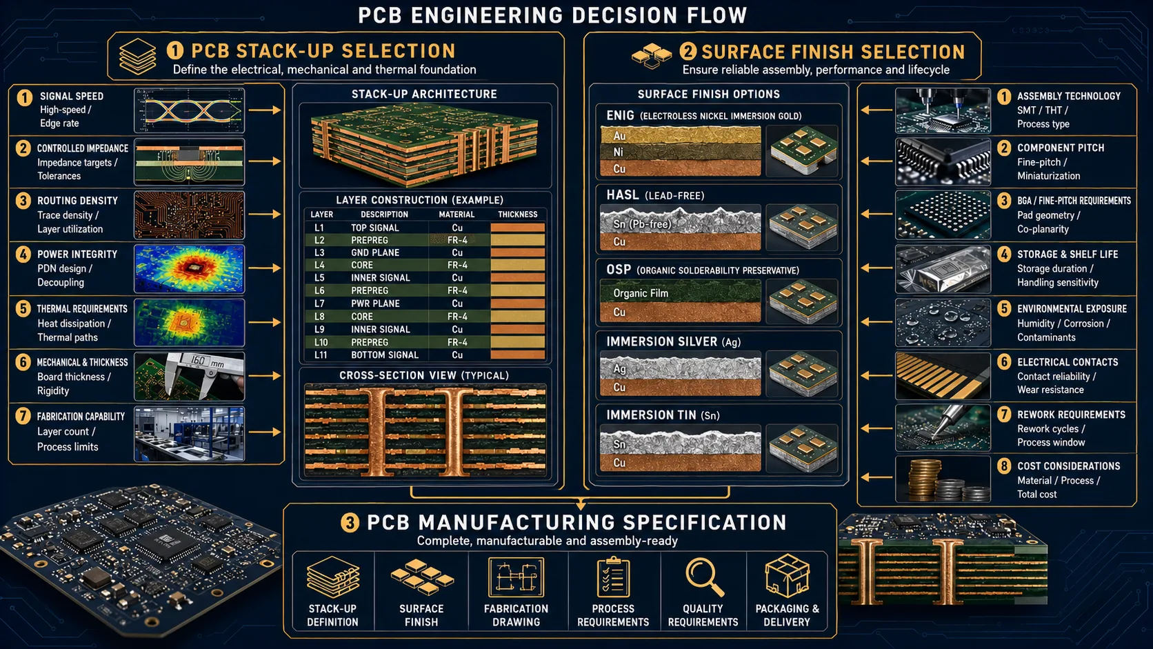
Step 1
Identify the assembly technology.
Step 2
Identify component pitch.
Step 3
Determine whether BGA/fine-pitch devices are present.
Step 4
Determine storage requirements.
Step 5
Determine environmental exposure.
Step 6
Determine whether electrical contacts are required.
Step 7
Evaluate rework requirements.
Step 8
Compare cost and manufacturing availability.
Step 9
Specify the exact finish in the fabrication documentation.
39. Common Stack-Up Mistakes
Mistake 1: Choosing layer count first
Layer count should follow routing and electrical requirements.
Mistake 2: Ignoring reference planes
High-speed signals need controlled return paths.
Mistake 3: Using generic impedance assumptions
Actual impedance depends on physical construction.
Mistake 4: Ignoring fabrication tolerances
The theoretical geometry must be manufacturable.
Mistake 5: Treating FR-4 as one universal material
Material properties vary between constructions.
Mistake 6: Crossing reference-plane discontinuities
This can compromise return-current behavior.
Mistake 7: Ignoring copper thickness
Copper geometry influences both impedance and current capability.
40. Common Surface-Finish Mistakes
Mistake 1: Selecting finish based only on price
The cheapest finish may not be appropriate for the assembly.
Mistake 2: Confusing ENIG with hard gold
They serve different purposes.
Mistake 3: Using HASL for every application
Fine-pitch requirements may favor a flatter finish.
Mistake 4: Ignoring storage conditions
Some finishes require more controlled handling and storage.
Mistake 5: Ignoring contact requirements
Electrical-contact applications may require a different plating construction.
Mistake 6: Leaving finish unspecified
“Gold PCB” is not a sufficiently precise manufacturing specification.
41. Procurement Considerations
Procurement teams should not evaluate a PCB quotation without checking whether suppliers are quoting the same technical construction.
Two quotations can differ because one supplier is using:
The apparently cheaper quotation may therefore not be technically equivalent.
For meaningful comparison, normalize the specification first.
42. What Should Be Included in the RFQ?
A professional PCB RFQ should ideally define:
Board construction
Electrical
Fabrication
Assembly
Commercial
This prevents suppliers from quoting different technical interpretations.
43. A Simple Engineering Comparison
| Requirement | Stack-Up Consideration | Surface-Finish Consideration |
|---|---|---|
| High-speed signaling | Layer geometry, reference planes, impedance | Usually secondary |
| Fine-pitch SMT | Routing/escape geometry | Planarity becomes important |
| BGA | Layer count, via/escape strategy | Flat soldering surface important |
| High current | Heavy copper, planes | Application dependent |
| RF | Controlled geometry, reference planes | Application dependent |
| Edge connector | Mechanical construction | Contact plating becomes critical |
| Long storage | Material/environmental design | Finish stability important |
| High-volume SMT | Manufacturing efficiency | Cost + assembly compatibility |
| Harsh environment | Material and construction | Finish/environmental suitability |
44. The Best Stack-Up Is Not the Most Complex One
A sophisticated PCB does not necessarily require:
unless the product requires them.
Every additional fabrication complexity introduces cost and manufacturing considerations.
The best stack-up is therefore:
The simplest manufacturable construction that satisfies the electrical, mechanical, thermal and reliability requirements.
45. The Best Surface Finish Is Not the Most Expensive One
Similarly, ENIG is not automatically “better” than every other finish.
A surface finish should be selected based on:
For some products, OSP or lead-free HASL may be entirely appropriate.
For others, ENIG may be the better fit.
The engineering requirement should determine the finish.
46. When to Involve the PCB Manufacturer
Bring the manufacturer into the discussion when:
Early collaboration can prevent a design that is electrically attractive but difficult or expensive to manufacture.
47. From Design Intent to Manufacturing Reality
A good PCB specification bridges three domains:
Design intent
What the engineer needs electrically.
Manufacturing capability
What the fabricator can reliably build.
Commercial requirement
What the customer can economically produce.
The optimal PCB is where these three overlap.
48. Final Engineering Checklist
Before releasing a PCB design for fabrication, confirm:
Stack-Up
☐ Layer count is justified
☐ Signal/reference-plane relationships are appropriate
☐ Controlled-impedance structures are defined
☐ Copper thickness is defined
☐ Dielectric construction is appropriate
☐ Finished board thickness is defined
☐ Via technology is manufacturable
☐ Stack-up has been reviewed against fabrication capability
Surface Finish
☐ Finish is explicitly specified
☐ Fine-pitch/BGA requirements are considered
☐ Storage requirements are understood
☐ Environmental conditions are considered
☐ Contact-plating requirements are identified
☐ Finish is compatible with assembly
☐ Cost has been evaluated
Manufacturing
☐ DFM review completed
☐ Impedance requirements communicated
☐ Fabricator has confirmed manufacturability
☐ Fabrication drawing is complete
☐ Revision status is controlled
49. Conclusion
Selecting a PCB stack-up and surface finish should never be reduced to choosing from a standard menu.
The stack-up determines the physical relationship between:
signals
reference planes
power distribution
dielectric structures
copper
and ultimately influences signal integrity, impedance, thermal behavior and manufacturability.
Surface finish solves a different problem. It protects exposed copper and provides the appropriate surface for soldering or electrical contact, with the right choice depending on:
assembly technology
component geometry
storage
environment
reliability
contact requirements
and cost.
For a professional PCB manufacturing program, the decision should therefore follow a disciplined sequence:
Define electrical requirements → engineer the stack-up → validate impedance and manufacturability → select the surface finish → confirm assembly compatibility → finalize the manufacturing specification.
The goal is not the most sophisticated PCB construction or the most expensive surface finish.
It is the right construction for the product, the application and the manufacturing process.
Frequently Asked Questions
Ready to manufacture your electronics project?
Upload your Gerber files & BOM for automated DFM review, engineering feedback, and guaranteed delivery timelines.