Common DFM Issues in PCB Design
A Practical Guide to Identifying and Preventing Manufacturing Risks Before PCB Fabrication, Assembly and Production
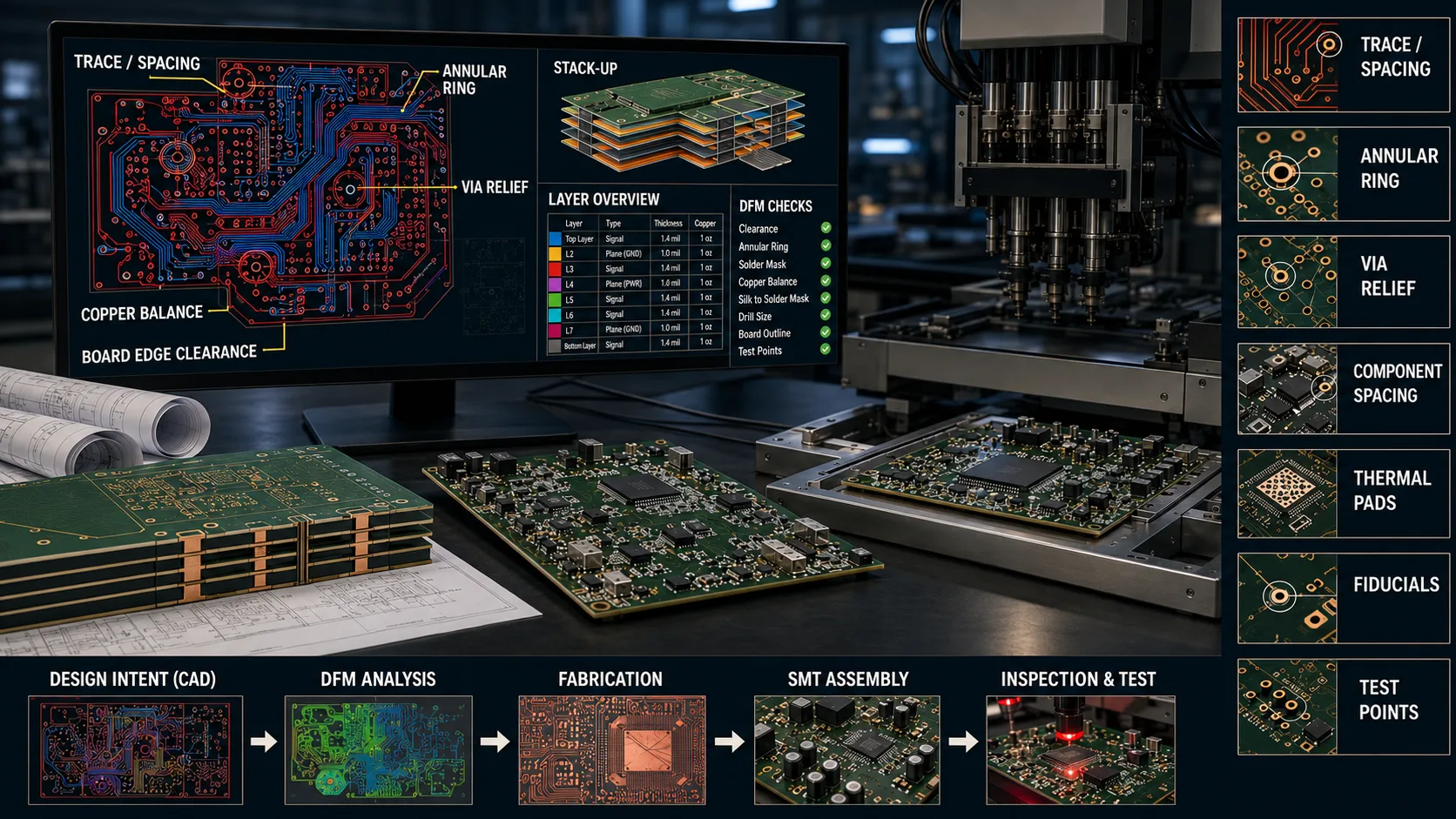
Common DFM Issues in PCB Design: What Engineers Should Check Before Manufacturing
A PCB can be electrically correct and still be difficult, expensive or unreliable to manufacture.
A schematic can pass electrical checks. A layout can pass CAD design-rule checks. Gerber files can generate correctly. A prototype can even work.
Yet the design may still create problems when it reaches fabrication, assembly, inspection, testing or volume production.
These problems can appear as:
fabrication constraints
assembly defects
lower manufacturing yield
additional engineering iterations
production delays
unexpected cost
inspection difficulties
inaccessible test points
supplier-specific manufacturing issues
or inconsistent production results
This is the purpose of Design for Manufacturing (DFM).
DFM asks a broader question than simply whether a PCB can be routed or whether CAD rules have been satisfied:
Can this design be fabricated, assembled, inspected and tested repeatedly within the capabilities of the intended manufacturing process?
That distinction becomes especially important when a design moves from prototype to production or from one manufacturing supplier to another.
1. What Is DFM in PCB Design?
Design for Manufacturing is the practice of evaluating a PCB against the actual capabilities, processes and tolerances of the manufacturing operation that will produce it.
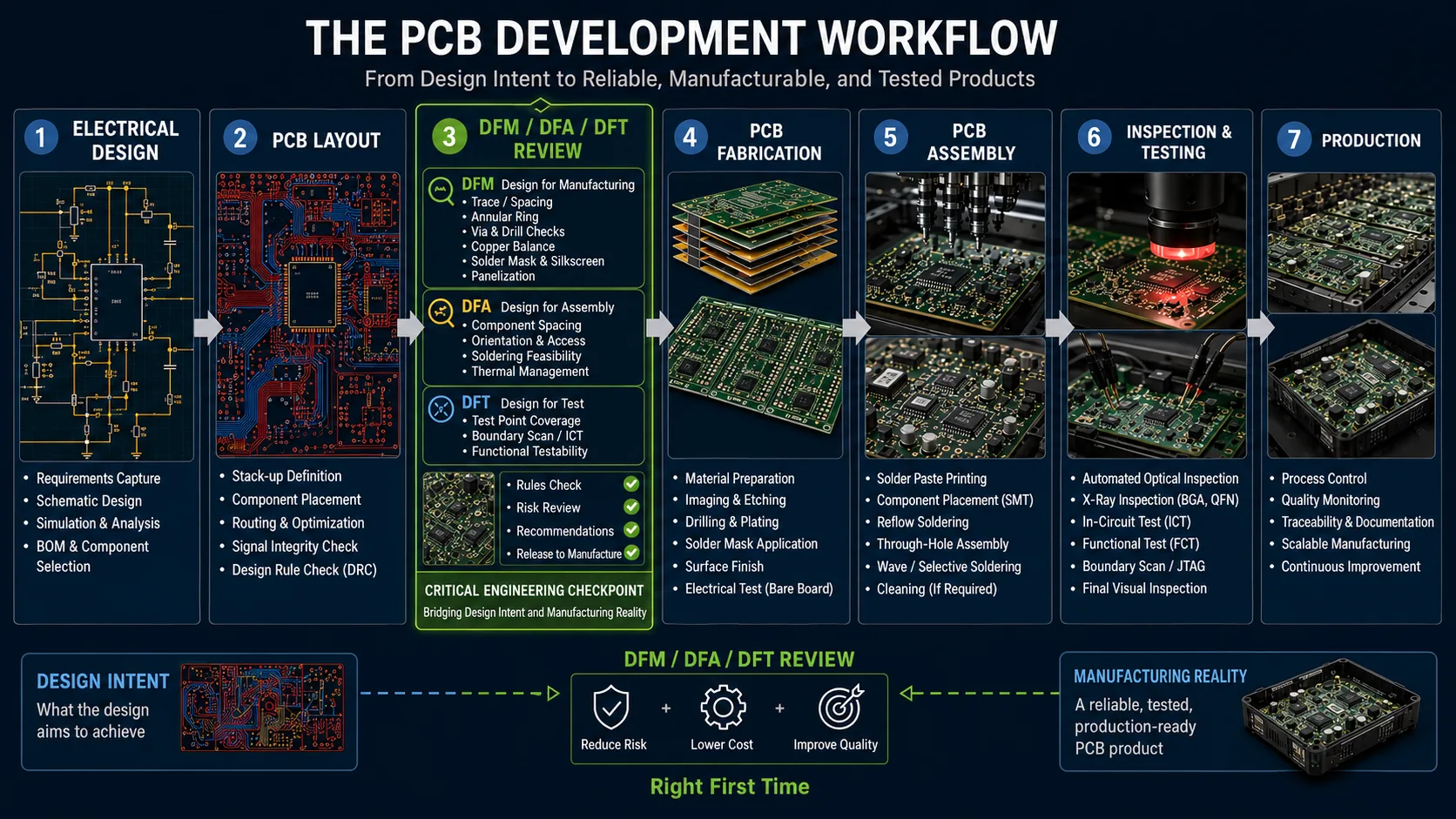
A simplified production path is:
Electrical Design
↓
PCB Layout
↓
DFM / DFA / DFT Review
↓
Fabrication
↓
Assembly
↓
Inspection & Testing
↓
Production
A DFM review therefore goes far beyond checking trace width.
It can include:
trace width and spacing
drill sizes
annular rings
via structures
copper-to-edge clearance
copper distribution
stack-up
material selection
solder-mask clearances
silkscreen
component footprints
component spacing
thermal pads
fiducials
panelization
test-point accessibility
assembly clearances
manufacturing tolerances
production documentation
The exact requirements depend on the PCB technology and the actual manufacturing process.
2. DRC Passed Does Not Mean DFM Passed
One of the most common misconceptions is that a PCB is production-ready because it passes a design-rule check.
A CAD DRC typically checks rules configured in the design environment, such as:
minimum trace width
minimum spacing
electrical clearance
routing constraints
via rules
connectivity
DFM asks a different question:
Can the actual manufacturer repeatedly build this specific design with sufficient process margin?
A design can therefore be DRC-clean but still require DFM corrections.
The distinction is important:
DRC | DFM |
|---|---|
Checks configured CAD rules | Checks real manufacturing capability |
Primarily design-environment focused | Manufacturing-process focused |
May use generic constraints | Uses supplier/process-specific capability |
Checks whether rules are satisfied | Checks whether production is practical and repeatable |
This is one of the most important concepts for engineering and procurement teams to understand.
3. Designing Directly at the Manufacturer's Absolute Limits
A manufacturer may advertise a minimum capability for:
trace width
spacing
drill diameter
annular ring
copper-to-edge clearance
via structures
That does not mean those limits should automatically become the design target.
There is an important difference between:
Theoretical capability
and
Preferred production capability with process margin.
A design operating permanently at the edge of a process window can be more sensitive to:
etching variation
drilling variation
registration variation
plating variation
material variation
process drift
Where electrical and mechanical requirements permit it, maintaining reasonable manufacturing margin can improve robustness and supplier flexibility.
4. Trace Width and Spacing
Trace width and trace-to-trace spacing are fundamental DFM considerations.
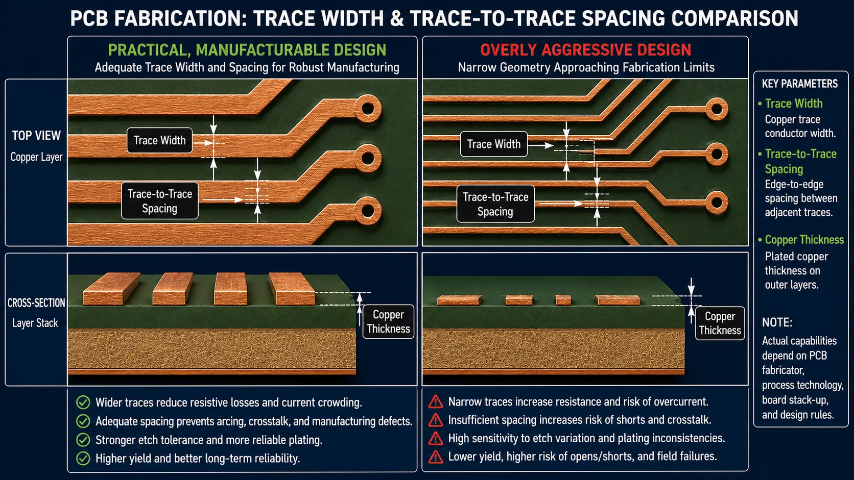
Very fine geometry can increase:
imaging and etching sensitivity
risk of opens
risk of shorts
fabrication complexity
cost
supplier restrictions
yield sensitivity
The right question is therefore not:
"What is the smallest geometry my CAD system allows?"
It is:
"What geometry satisfies the electrical requirements while retaining a practical manufacturing margin?"
The actual requirement depends on factors such as:
copper thickness
PCB layer
material
fabrication technology
impedance requirements
production volume
5. Drill Size, Annular Rings and Via Structures
Vias are essential to multilayer PCB design, but their geometry must be compatible with fabrication capabilities.
DFM review should consider:
finished hole diameter
drill-tool diameter
pad diameter
annular ring
drill-to-copper clearance
via-to-via spacing
via-to-pad relationships
layer transitions
fabrication tolerances
An annular ring provides copper around a drilled hole. If the drill is not perfectly centered because of normal manufacturing variation, sufficient annular ring provides additional tolerance.
Advanced structures such as:
blind vias
buried vias
microvias
stacked microvias
sequentially laminated structures
require even closer alignment between the design and the manufacturing process.
The CAD tool may support an advanced via structure; that does not automatically mean the intended supplier can produce it reliably.
6. Stack-Up Must Match Manufacturing Reality
The PCB stack-up affects much more than layer count.
It influences:
dielectric thickness
impedance
signal integrity
power integrity
copper distribution
via structures
overall board thickness
mechanical construction
This becomes particularly important for:
high-speed digital designs
RF boards
differential pairs
controlled-impedance designs
high-current designs
If the PCB is routed using one assumed stack-up but manufactured using another, the resulting electrical characteristics may differ from the original design intent.
For controlled-impedance boards, the stack-up should therefore be treated as an engineering parameter, not simply a procurement detail.
7. Copper Distribution and Board Balance

Copper distribution should be considered alongside stack-up and fabrication process capability.
Highly unbalanced copper distribution can create manufacturing challenges involving:
plating
etching
dimensional variation
thermal behavior
board flatness
warpage
This does not mean every PCB must have perfectly symmetrical copper.
Rather, the copper distribution should be evaluated as part of the complete fabrication process.
For multilayer boards, copper balancing between layers can also be important.
8. Board-Edge Clearance and Panelization
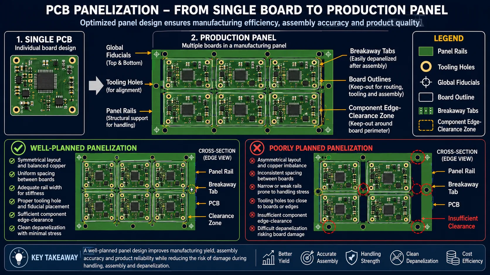
Panelization affects tooling, assembly handling, depanelization and production efficiency and should be considered early.
Copper and components positioned too close to the PCB edge can create manufacturing problems.
The design should consider:
copper-to-edge clearance
component-to-edge clearance
plated holes near edges
connectors
V-scoring
routing
depanelization
tooling
panel rails
A PCB is also rarely manufactured as an isolated rectangle.
Production panels can include:
multiple boards
rails
tooling holes
fiducials
breakaway tabs
routing features
edge-clearance zones
Therefore, a PCB that looks perfectly acceptable as an individual board may present problems once placed into a production panel.
9. Assembly DFM: Footprints, Spacing and Thermal Pads
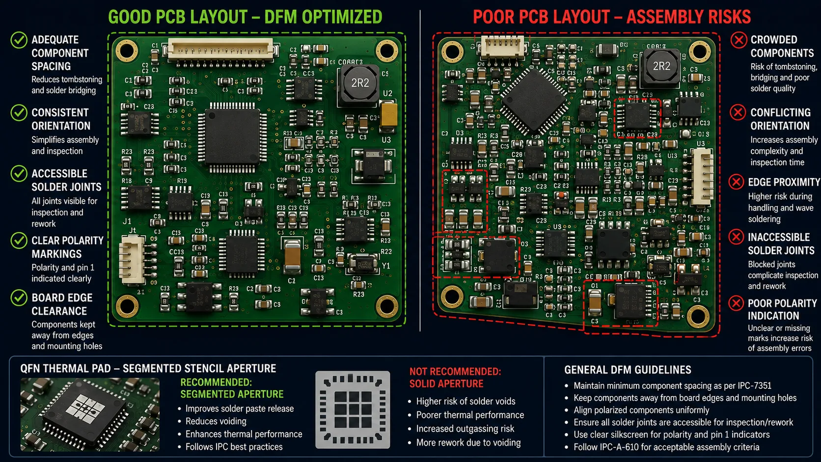
Assembly DFM addresses whether components can be placed, soldered, inspected and reworked reliably.
DFM does not stop at PCB fabrication.
A board can be completely fabricable and still be difficult to assemble.
Assembly DFM should consider:
component footprints
component spacing
package orientation
component height
pick-and-place access
solder-joint accessibility
inspection
rework
polarity markings
board-edge clearance
thermal interactions
Incorrect footprints can be especially problematic for:
QFN
DFN
BGA
LGA
fine-pitch QFP
bottom-termination components
Thermal pads also deserve attention.
A large uninterrupted solder-paste aperture can deposit excessive solder beneath an exposed-pad component. Depending on the package and process, segmented stencil apertures or paste-volume control may be required.
PCB layout and stencil design should therefore be considered together.
10. BGA, Fine-Pitch Components and Inspection
BGA and fine-pitch components introduce multiple interconnected DFM considerations.
These can include:
pad geometry
solder-mask strategy
escape routing
via placement
assembly tolerances
solder-joint inspection
X-ray requirements
rework access
Because many BGA solder joints are hidden underneath the package, inspection strategy must be considered alongside the design.
Depending on the product and process, inspection may involve:
AOI for visible features
X-ray inspection
electrical testing
functional testing
process monitoring
The important point is that a BGA should be evaluated as part of the complete manufacturing and inspection strategy, not merely as a footprint.
11. Fiducials, Component Orientation and Automated Assembly
Automated SMT equipment relies on optical recognition and alignment.
Appropriate fiducials can help machine-vision systems establish accurate board and component positioning.
Consider:
global fiducials
local fiducials where appropriate
panel fiducials
unobstructed visibility
consistent placement
Component orientation also matters.
Consistent orientation of:
polarized components
diodes
LEDs
ICs
connectors
can improve machine programming, inspection, polarity verification and troubleshooting.
12. Solder Mask and Silkscreen Problems
Solder-mask design affects pad definition and solderability.
Potential problems include:
inadequate pad exposure
solder-mask slivers
registration concerns
exposed copper
solder bridging
manufacturing limitations on fine-pitch features
Silkscreen problems are less dramatic but still important.
Common examples include:
reference designators over pads
polarity markings hidden beneath components
markings extending beyond board edges
overlapping component outlines
Good silkscreen design improves assembly interpretation, inspection and serviceability.
13. DFM Must Include Testability
A PCB can function electrically and still be difficult to test in production.
DFT—or Design for Testability—should be considered alongside DFM and DFA.
Depending on the product, test access may be required for:
power rails
ground
communication interfaces
programming interfaces
critical signals
analog nodes
functional test interfaces
A test point that exists electrically but is physically inaccessible may have little practical value.
Consider:
probe clearance
component obstruction
connector interference
bottom-side access
fixture access
enclosure restrictions
Test strategy should therefore be considered during layout rather than added after the board is complete.
14. Manufacturing Data Must Be Complete and Consistent
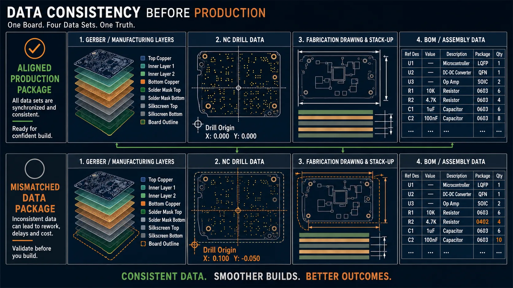
Every manufacturing file should describe the same approved product revision consistently.
A good PCB layout can still fail at manufacturing release if the production package is incomplete or inconsistent.
Typical fabrication information includes:
Gerber or other manufacturing data
NC drill files
fabrication drawing
stack-up
material
surface finish
impedance requirements
board dimensions
tolerances
Assembly information may include:
BOM
pick-and-place data
assembly drawing
paste layers
polarity information
component references
More importantly, these files must describe the same approved product revision.
Potential problems include:
Gerber layer count not matching the drawing
inconsistent board outlines
different drill origins
mismatched drill units
BOM revision differing from PCB revision
inconsistent component references
conflicting polarity information
These inconsistencies can result in manufacturing holds and clarification cycles before production even begins.
15. BOM and Component Lifecycle Are Part of DFM
One of the most valuable additions from the overseas-production article is the recognition that DFM should not be isolated from the BOM.
Component selection can influence:
package type
placement
soldering
assembly complexity
sourcing
lead time
lifecycle
alternate availability
A PCB can therefore be physically manufacturable but commercially difficult to produce.
Consider components that are:
unusual
single-source
long-lead
NRND
obsolete
difficult to substitute
For long-life products, component lifecycle should be evaluated before production release.
This is particularly important for industrial, medical, automotive and infrastructure products.
16. Supplier Capability Is Part of the DFM Equation
DFM is not completely supplier-independent.
A board successfully manufactured by Supplier A does not necessarily have identical manufacturing risk at Supplier B.
Differences can exist in:
trace/space capability
drilling
via technology
materials
stack-up
impedance control
surface finish
SMT placement
inspection
testing
panelization
Therefore:
DFM should ultimately be validated against the actual manufacturing process that will produce the board.
This is especially important when transferring production to a new supplier or sourcing internationally.
17. Why Overseas Production Requires Better Manufacturing Alignment
The technical principles of DFM do not change simply because production crosses a border.
What can change is the number of organizations, assumptions and process interfaces involved.
For an overseas project:
Design team↓Procurement / sourcing↓PCB fabricator↓PCB assembler↓Inspection / test↓Logistics
Each handoff creates an opportunity for assumptions to become misaligned.
That makes clear documentation, supplier-specific capability review, revision control and early engineering communication especially important.
The objective is not to design differently merely because production is overseas.
The objective is to ensure that everyone is working from the same technical definition of the product.
18. Don't Optimize the Design Only for the Lowest Quotation
A technically cheaper quotation does not automatically represent the lowest manufacturing risk.
For example, one supplier may quote a lower initial price but require:
tighter process assumptions
unusual material
special fabrication steps
longer lead time
Another supplier may have a somewhat higher unit price but offer:
more conventional construction
better material availability
greater process margin
simpler production
stronger supply continuity
This is why DFM should be connected to total manufacturing cost and supply-chain stability, not simply the first unit-price comparison.
19. Prototype DFM Is Not Production DFM
A prototype that works is not necessarily production-ready.
A prototype may have been:
manually assembled
built in very small quantities
heavily inspected
manually reworked
produced using a different process
Production introduces additional requirements:
repeatability
yield
automated assembly
inspection throughput
test coverage
panel efficiency
component availability
process capability
controlled documentation
The important question changes from:
"Does the prototype work?"
to:
"Can the design be manufactured repeatedly at the intended volume?"
20. DFM Should Be Iterative, Not a Final Gate
A mature DFM process does not wait until Gerbers are ready.
At schematic stage
Review:
component packages
lifecycle
special technologies
test requirements
During layout
Review:
geometry
clearances
routing
component placement
thermal design
Before fabrication
Review:
stack-up
panelization
tolerances
manufacturing data
Before assembly
Review:
BOM
footprints
paste
placement
fiducials
assembly constraints
Before production
Review:
inspection
testing
process capability
approved revisions
This iterative approach catches problems when they are still relatively easy to correct.
21. DFM, DFA and DFT Should Work Together
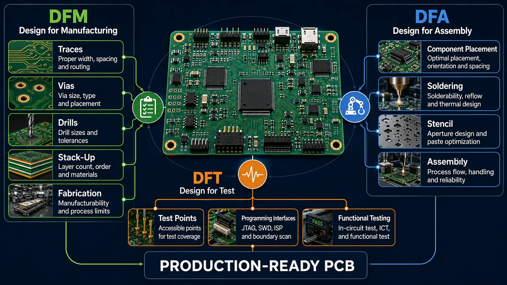
These disciplines are related but not identical.
DFM — Design for Manufacturing
Focuses primarily on PCB fabrication:
trace geometry
spacing
drills
vias
stack-up
tolerances
DFA — Design for Assembly
Focuses on:
component spacing
orientation
solderability
stencil considerations
inspection
rework
DFT — Design for Test
Focuses on:
test points
programming access
functional test interfaces
probe access
test coverage
A production-ready electronics design needs all three perspectives coordinated.
22. A Practical PCB DFM Release Checklist
Before releasing a design for manufacturing, review:
PCB Fabrication
☐ Trace width verified☐ Trace spacing verified☐ Drill sizes reviewed☐ Annular rings reviewed☐ Via structures reviewed☐ Copper-to-edge clearance checked☐ Board thickness confirmed☐ Copper thickness confirmed☐ Stack-up confirmed☐ Material confirmed☐ Surface finish confirmed☐ Controlled impedance requirements identified
Assembly
☐ Component footprints verified☐ Component spacing reviewed☐ Orientation reviewed☐ Polarity markings checked☐ BGA/QFN requirements reviewed☐ Thermal-pad design reviewed☐ Solder-mask clearances checked☐ Silkscreen reviewed☐ Fiducials considered☐ Panelization considered
Testing
☐ Test points identified☐ Probe accessibility checked☐ Programming access confirmed☐ Functional test strategy considered
Manufacturing Data
☐ Gerber/manufacturing data verified☐ NC drill files verified☐ Board outline verified☐ Fabrication drawing verified☐ BOM verified☐ Pick-and-place data verified☐ Assembly drawing verified☐ Revision consistency confirmed
Supply Chain
☐ MPNs validated☐ Component lifecycle checked☐ Long-lead components identified☐ Alternate sourcing considered☐ Production volume defined
Production
☐ Inspection requirements defined☐ Test requirements defined☐ Panelization reviewed☐ Packaging requirements defined☐ Lead time agreed☐ Engineering queries closed
The consolidated checklist retains the fabrication, assembly, testing and documentation coverage of the original DFM article while adding the BOM, supply-chain and production-release checks that were particularly useful in the overseas-production article.
23. What Should a Good DFM Review Actually Deliver?
A useful DFM review should not simply produce a long list of violations.
It should answer four fundamental questions:
Can the board be fabricated?
Are the geometry, materials, stack-up, drills and tolerances compatible with the process?
Can it be assembled?
Can components be placed, soldered, inspected and reworked reliably?
Can it be tested?
Are required signals, programming interfaces and test points accessible?
Can it be produced repeatedly?
Does the design provide enough manufacturing margin for the intended volume?
That final question is particularly important.
The goal is not necessarily zero DFM comments.
Some designs legitimately require:
HDI
fine-pitch components
controlled impedance
special materials
advanced fabrication processes
The goal is to ensure that every significant manufacturing constraint is understood, technically justified and commercially acceptable.
24. A Better DFM Release Workflow
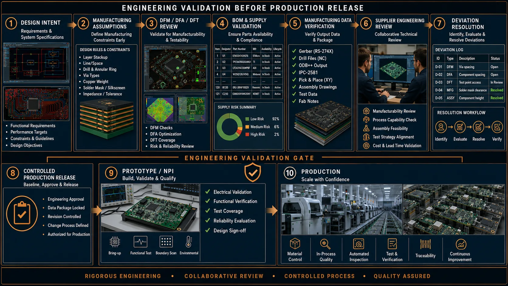
A structured DFM workflow connects design intent with manufacturing, supply-chain and production-release requirements.
A robust process can follow:
Define design intent-Electrical, mechanical, thermal and environmental requirements
↓
Define manufacturing assumptions-PCB technology, assembly technology, materials and testing
↓
Perform DFM / DFA / DFT review
↓
Validate BOM and component availability
↓
Validate manufacturing data
↓
Conduct supplier engineering review
↓
Resolve and document deviations
↓
Release the controlled production package
↓
Prototype / NPI
↓
Validate
↓
Production
This workflow combines the strongest production-readiness concepts from both source articles.
25. What Engineers and Procurement Teams Should Ask the Manufacturer
Before releasing a complex board, ask:
What are your preferred trace and spacing capabilities?
Are any design features operating close to your preferred process window?
Are the specified drill sizes and annular rings appropriate?
Is the proposed stack-up compatible with the required impedance?
Are the selected materials appropriate for the process?
Are special fabrication processes required?
Are component placement and package requirements compatible with assembly?
Are BGA and fine-pitch components compatible with the process?
Is the thermal-pad and stencil strategy appropriate?
Is the panelization strategy suitable?
Are test points accessible?
Are any BOM components difficult to source or nearing lifecycle risk?
Are there engineering assumptions behind the quotation?
Can the design be produced at the intended volume with adequate process margin?
What unresolved engineering questions must be closed before production?
These questions are particularly useful when qualifying a new supplier or moving an existing design into a new manufacturing environment.
26. Final Takeaway
A PCB is not production-ready simply because:
the schematic is correct,
the layout passes DRC,
the Gerbers generate successfully,
or the prototype works.
A production-ready PCB must also be:
Fabricable, Assemblable, Inspectable, Testable, Sourcable, Repeatable
within the capabilities of the intended manufacturing process.
The most useful DFM question is therefore not:
"Can this PCB be manufactured?"
It is:
"Can this PCB be manufactured repeatedly, at the required quality, volume, cost and lead time, using a clearly defined and controlled process?"
That is the difference between a PCB that is technically manufacturable and one that is genuinely production-ready.
27. A Practical DFM Review With QUADRIONIX
For engineering teams preparing a PCB for fabrication or PCBA production, DFM can serve as an important checkpoint before committing to manufacturing.
QUADRIONIX approaches the review from a broader manufacturability, assembly and production-risk perspective, helping identify potential issues involving PCB geometry, supplier capability, manufacturing data, assembly, testing and production readiness.
The objective is not simply to manufacture the board.
It is to create a controlled path from:
Design → DFM/DFA/DFT Review → Engineering Validation → Prototype/NPI → Production
with fewer avoidable manufacturing surprises.
What is DFM in PCB design?
DFM, or Design for Manufacturing, is the process of reviewing a PCB design against the capabilities and tolerances of the intended manufacturing process before production.
Is passing PCB DRC enough?
No. DRC verifies the rules configured in the CAD environment. DFM also considers actual fabrication, assembly, inspection, testing and production capabilities.
What are the most common PCB DFM issues?
Common issues include aggressive trace/spacing, insufficient annular rings, inappropriate drill sizes, poor copper distribution, inadequate board-edge clearance, poor component spacing, thermal-pad problems, missing fiducials, inaccessible test points and inconsistent manufacturing data.
Should DFM be done before Gerber release?
Yes. Ideally, manufacturability should be considered throughout design rather than being treated as a final check immediately before manufacturing.
Does DFM matter when changing PCB suppliers?
Yes. Different manufacturers can have different process windows, materials, stack-ups, equipment and inspection capabilities. A successful design at one supplier should therefore be reviewed before transfer to another.
Does DFM include BOM and component sourcing?
A broader production-readiness review should consider BOM characteristics such as package type, lifecycle, availability, lead time and alternate sourcing because these factors can affect assembly and production continuity.
Frequently Asked Questions
Ready to manufacture your electronics project?
Upload your Gerber files & BOM for automated DFM review, engineering feedback, and guaranteed delivery timelines.