BGA Assembly Challenges and How to Avoid Them
A practical guide to BGA PCB assembly, solder-joint reliability, inspection, reflow, warpage, voiding and manufacturing controls

BGA PCB assembly showing solder-ball array and SMT manufacturing process
Ball Grid Array, or BGA, packages have become essential for many modern electronic products.
They provide a large number of electrical connections within a relatively compact footprint, making them particularly useful for:
But BGA assembly introduces a fundamental manufacturing challenge:
The majority of solder joints are hidden underneath the component.
With conventional visible-lead packages, many solder joints can be inspected directly.
With a BGA, the solder connections exist between the underside of the package and the PCB.
That changes almost everything about inspection, process control and defect detection.
Reliable BGA assembly therefore depends on a combination of:
PCB design + pad design + stencil printing + component placement + reflow + inspection + process control
—not simply placing the BGA on the board.
1. What Makes BGA Assembly Different?
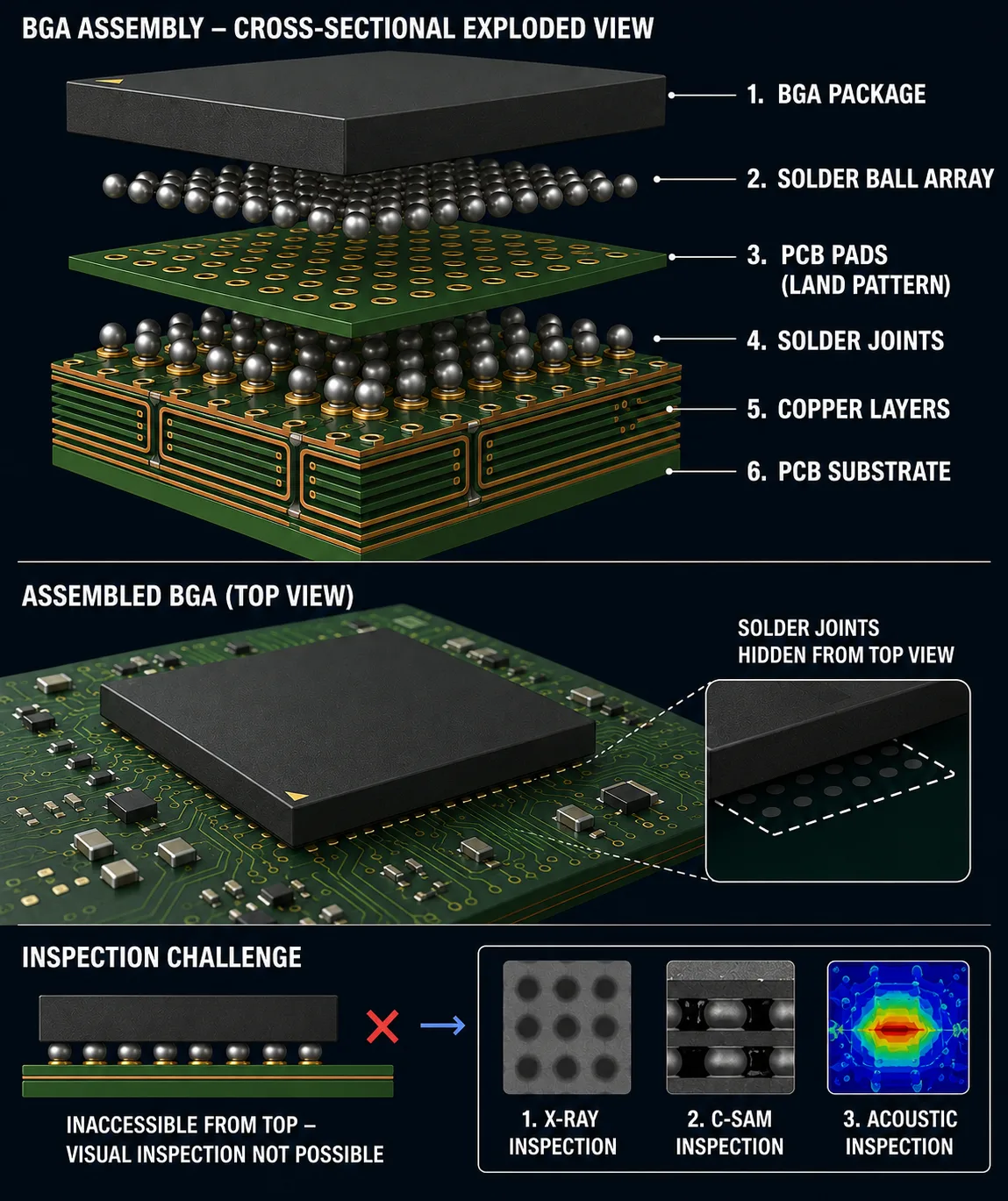
Unlike leaded packages, most BGA solder joints are hidden beneath the component after assembly.
A BGA component has an array of solder balls arranged beneath the package.
During SMT assembly, the component is placed onto corresponding PCB pads.
The assembly then passes through the reflow process.
The solder balls melt and form electrical and mechanical connections between:
BGA package ↔ solder joint ↔ PCB pad
The challenge is that these connections are largely hidden after assembly.
This means a manufacturing defect can potentially remain invisible from the top of the PCB.
2. Common BGA Assembly Challenges
The most important BGA manufacturing challenges include:
These problems are interconnected.
For example, a BGA soldering problem may not originate at the BGA itself.
It could begin with:
Stencil design → paste deposition → component placement → reflow
This is why BGA quality requires process-level thinking.
3. Solder Paste Printing Is Critical
Before the BGA is placed, solder paste must be deposited accurately onto the PCB pads.
For fine-pitch BGA packages, the process window can become significantly narrower.
Variables include:
Insufficient paste can contribute to weak or open joints.
Excessive paste can increase the risk of bridging or other solder-related defects.
Therefore:
BGA reliability starts before the component reaches the placement machine.
4. Stencil Design Matters
BGA pad geometry and pitch influence the stencil design.
The objective is to achieve consistent solder-paste volume across the entire BGA footprint.
For fine-pitch devices, designers and manufacturers may need to evaluate:
The correct solution depends on the package and overall PCB assembly design.
A generic stencil rule should not replace engineering evaluation.
5. Component Placement Accuracy
BGA placement requires sufficient positional accuracy so that the solder-ball array aligns correctly with the PCB land pattern.
Modern placement equipment uses vision systems to assist alignment.
However, accurate placement alone does not guarantee a reliable BGA joint.
The final result still depends on:
6. Reflow Profile Control
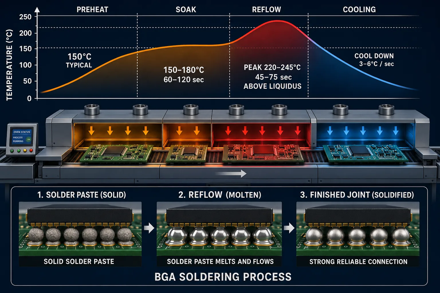
A controlled thermal profile helps create consistent solder-joint formation across the BGA footprint.
Reflow is one of the most important stages in BGA assembly.
The PCB assembly passes through controlled thermal zones where the solder paste undergoes a sequence of heating and cooling stages.
The profile needs to be compatible with:
A poorly controlled profile can result in:
7. BGA Thermal Imbalance
Large BGAs can have significant thermal mass.
Different areas of the PCB may also heat at different rates.
This can create thermal gradients across the assembly.
For example, the center of a large BGA may behave differently from its outer edges during heating and cooling.
The manufacturing process therefore needs to account for:
8. Head-in-Pillow Defects
One important BGA defect is commonly known as head-in-pillow.
It can occur when the solder ball and solder paste do not form a proper metallurgical connection during reflow.
Visually, the solder may appear to have contacted the pad and ball, but the actual joint can remain electrically unreliable.
Factors that may contribute include:
Because the defect occurs underneath the BGA, conventional visual inspection may not detect it reliably.
9. BGA Voiding
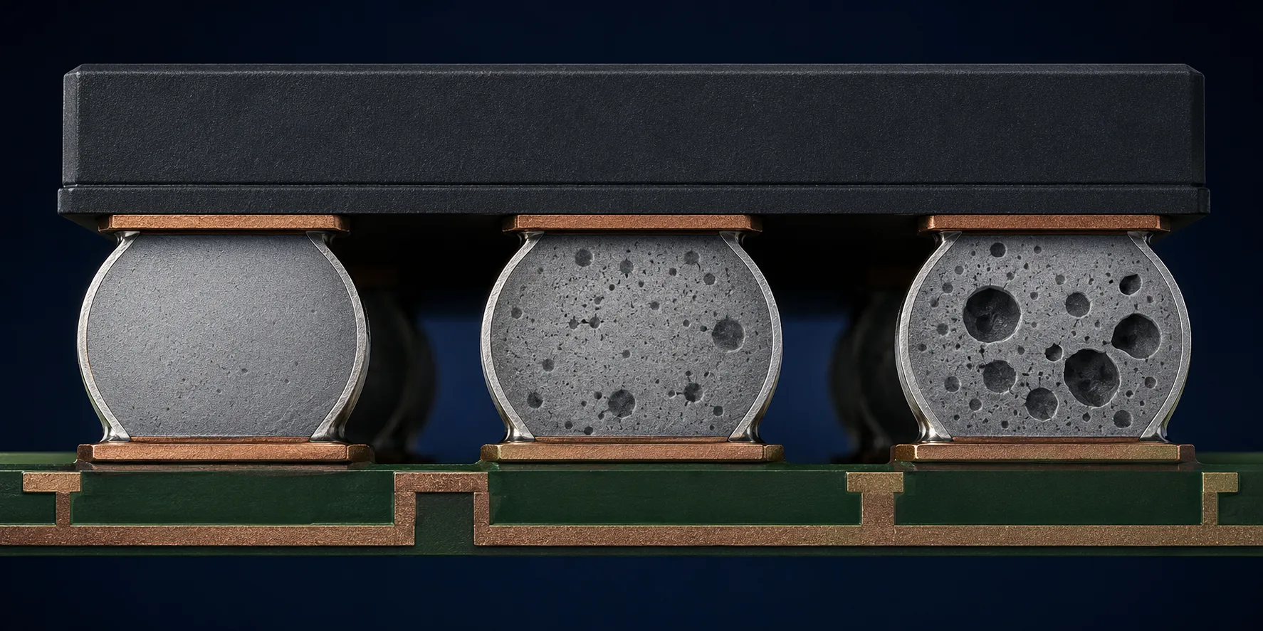
X-ray inspection can reveal internal solder-joint features that cannot be seen from the PCB surface.
Voids are areas within a solder joint where gas or other material prevents complete solder continuity.
Some degree of voiding can occur in many solder joints.
The engineering question is:
Is the level and distribution of voiding acceptable for the particular application?
Voiding can be influenced by:
For certain applications, especially those involving thermal or high-current requirements, voiding may deserve particular attention.
10. PCB Warpage Can Affect BGA Reliability
A PCB must remain sufficiently flat during assembly.
Excessive warpage can affect:
Large multilayer boards, asymmetric copper distribution and thermal stress can contribute to warpage.
BGA assembly therefore benefits from good PCB construction and process control.
11. Package Warpage Matters Too
The PCB is not the only source of deformation.
BGA packages themselves can exhibit thermal or mechanical warpage.
During reflow, the package may respond differently from the PCB.
This can affect the contact between solder balls and PCB pads.
This is particularly important for larger packages and fine-pitch devices.
12. Pad Design and Land Pattern
BGA reliability begins partly at the PCB design stage.
The PCB footprint should follow the component manufacturer's recommended land pattern wherever appropriate.
Important considerations include:
A footprint that is technically possible but poorly optimized for manufacturing can create unnecessary assembly risk.
13. Via-in-Pad Requires Careful Control
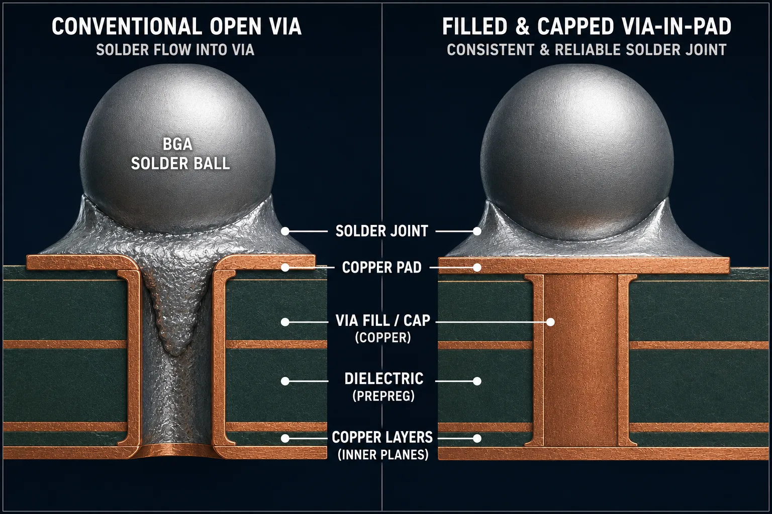
Via-in-pad technology can support high-density BGA routing, but the via structure must be appropriate for the assembly process.
For high-density BGA designs, vias may need to be positioned within or very close to the BGA pads.
This can enable compact routing.
However, conventional open vias in pads can create solder-management problems because solder may flow into the via.
Depending on the design, manufacturers may use technologies such as:
The appropriate technology depends on the PCB design and manufacturing requirements.
14. Surface Finish Can Influence Assembly
The PCB surface finish forms part of the soldering interface.
Common finishes include:
The appropriate finish depends on the design, package, pitch, reliability requirements and manufacturing process.
For fine-pitch BGA assembly, a uniform and suitable surface finish is particularly important.
15. Why AOI Alone Is Not Enough for BGA
Automated Optical Inspection, or AOI, is extremely useful for SMT assembly.
However, most BGA solder joints are hidden underneath the package.
Therefore, conventional top-side optical inspection cannot directly inspect every BGA solder connection.
AOI can still be useful for inspecting:
But additional inspection methods may be needed for the BGA itself.
16. Why X-Ray Inspection Is Important
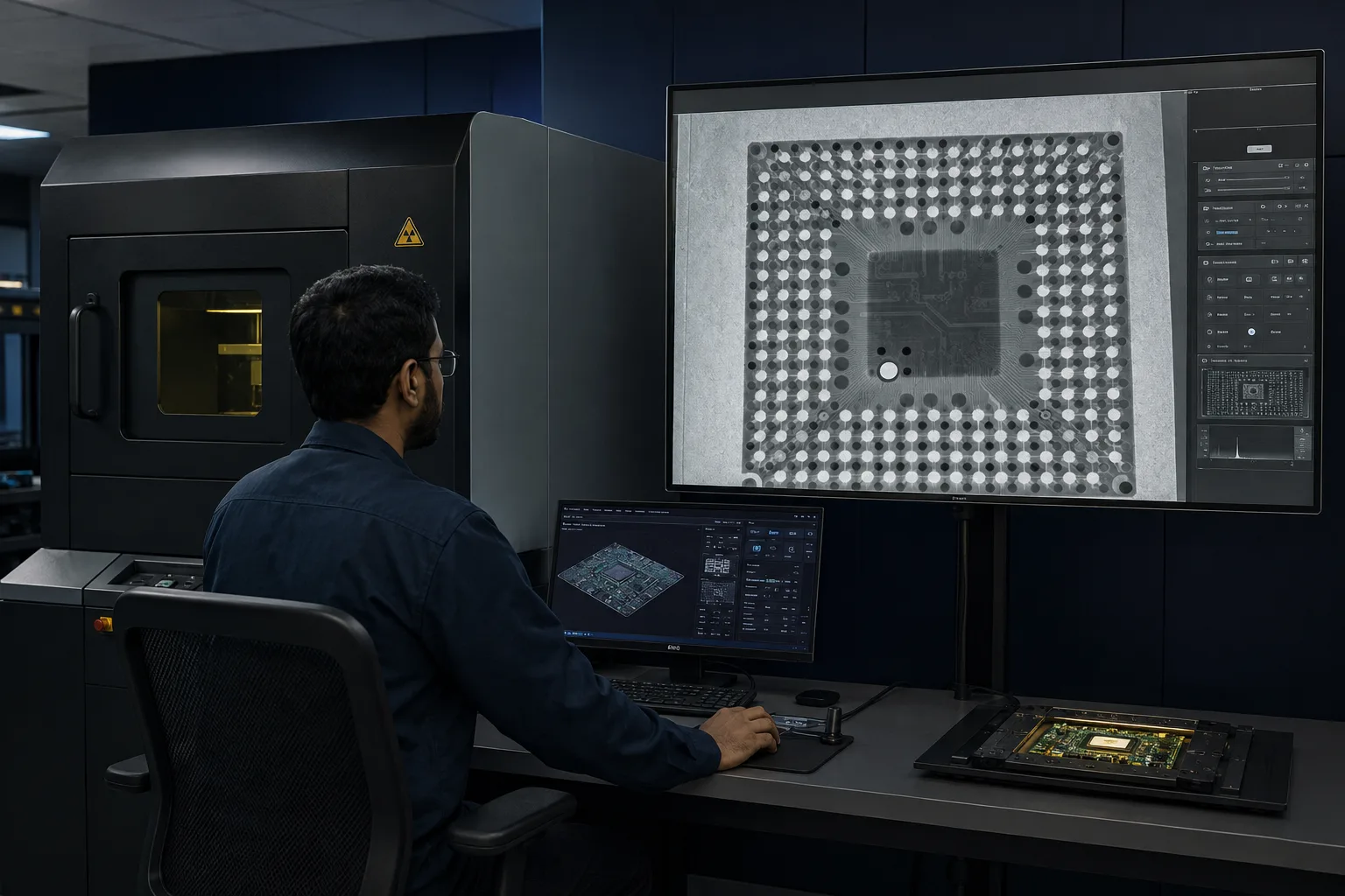
X-ray inspection provides visibility into BGA solder joints that remain hidden beneath the package.
X-ray inspection allows manufacturers to examine structures that are hidden from conventional optical inspection.
Depending on the system and application, X-ray inspection can help identify:
For BGA-heavy assemblies, X-ray capability can therefore be an important supplier-selection criterion.
17. X-Ray Is a Tool—Not a Substitute for Process Control
Inspection identifies defects.
It does not necessarily prevent them.
A strong BGA manufacturing process therefore combines:
Design controls
Stencil and printing controls
Placement controls
Reflow controls
Inspection
Process improvement
The objective should be to reduce the probability of defects rather than simply find them after production.
18. BGA Rework Is More Difficult
When a BGA fails inspection, rework is more complicated than replacing a visible-lead component.
The process may involve:
Repeated thermal cycles can also introduce additional stress.
For high-value assemblies, minimizing unnecessary BGA rework is therefore important.
19. Moisture and Component Handling
Some semiconductor packages are moisture-sensitive.
Improper storage or handling can introduce reliability risks during reflow.
Manufacturers should therefore follow the relevant component handling and moisture-sensitivity requirements supplied by the component manufacturer.
Good controls may include:
This is particularly important for sensitive BGA packages.
20. BGA Assembly Is Also an NPI Challenge
A BGA design that works in a prototype does not automatically guarantee smooth volume production.
During NPI, the manufacturer should evaluate:
This is where early manufacturing involvement can prevent expensive production-stage problems.
21. Common BGA Defects and Potential Causes
| Defect | Possible contributing factors |
|---|---|
| Open solder joint | Insufficient paste, warpage, placement or reflow issues |
| Head-in-pillow | Package/PCB warpage, oxidation, thermal-profile issues |
| Bridging | Excessive paste, stencil design or alignment |
| Voiding | Paste chemistry, printing and reflow conditions |
| Misalignment | Placement or pad-design issues |
| Poor wetting | Surface condition, oxidation or process issues |
| Solder balling | Paste/process conditions |
| Excessive solder | Stencil or paste-deposition issues |
| Pad-related defects | Footprint or PCB fabrication issues |
These causes are not universal diagnoses. A proper root-cause investigation should consider the actual assembly process and evidence from inspection.
22. A Practical BGA Manufacturing Control Plan

Reliable BGA assembly is a controlled process spanning design, printing, placement, reflow, inspection and continuous improvement.
A robust process can be organized into six stages.
Stage 1 — Design Review
Check:
Stage 2 — Stencil Review
Check:
Stage 3 — SMT Placement
Verify:
Stage 4 — Reflow
Validate:
Stage 5 — Inspection
Use an appropriate combination of:
Stage 6 — Feedback
Use inspection results to improve:
23. Questions to Ask a BGA Assembly Supplier
If you are evaluating a PCB/PCBA manufacturing partner, ask:
Manufacturing Capability
Reflow
Inspection
NPI
Quality
These questions can reveal much more about a supplier's actual capability than simply asking:
"Can you assemble BGA?"
24. BGA Capability Is More Than Machine Capability
A supplier may have an SMT placement machine capable of placing BGA packages.
That does not automatically mean the supplier has a mature BGA manufacturing process.
Reliable BGA assembly depends on the entire system:
Equipment
Process engineering
Stencil technology
Reflow control
Inspection
Quality systems
Experienced operators and engineers
NPI discipline
This distinction is important when evaluating a manufacturing partner for production hardware.
25. BGA Assembly Checklist for Buyers
Before selecting a supplier, confirm:
26. How to Reduce BGA Assembly Risk
The most effective approach is to address risk early.
Before PCB fabrication
Review:
Footprint → stack-up → pad design → via strategy
Before assembly
Review:
Stencil → paste → component condition → placement
During NPI
Review:
Reflow → inspection → defect data → process capability
Before volume production
Review:
Yield → reliability → repeatability → documentation
This approach transforms BGA assembly from a reactive defect-management exercise into a controlled manufacturing process.
27. Final Takeaway
BGA packages enable high-density, high-performance electronic designs—but they also introduce manufacturing complexity because the majority of solder joints are hidden beneath the package.
Reliable BGA assembly depends on controlling the complete process:
→ PCB Design
→ Stencil & Paste
→ Placement
→ Reflow
→ Inspection
→ Verification
→ Continuous Improvement
The most important lesson for both engineers and sourcing teams is this:
Do not evaluate BGA capability based solely on whether a supplier owns an SMT placement machine. Evaluate the entire process required to consistently produce and verify hidden BGA solder joints.
A capable manufacturing partner should be able to demonstrate not only equipment capability, but also engineering review, process control, X-ray inspection, NPI discipline and production-quality management.
28. QUADRIONIX PERSPECTIVE
At QUADRIONIX, BGA assembly is treated as a complete manufacturing-engineering challenge rather than simply an SMT placement operation.
For BGA-intensive PCBA, the critical chain is:
→ Design review
→ DFM/DFA
→ Stencil optimization
→ Precision placement
→ Controlled reflow
→ X-ray inspection
→ Electrical verification
→ Production process control
This approach is particularly important when a BGA-based product moves from prototype → NPI → repeat production, where consistency and yield become increasingly important.
If you are Planning a BGA-based PCBA or Looking for a Reliable BGA PCBA Manufacturing Partner Quadrionix can review the assembly requirements from a DFM, process, inspection and production-readiness perspective before manufacturing.
From complex BGA assembly to production-ready PCBA — engineered for reliability
Frequently Asked Questions
Ready to manufacture your electronics project?
Upload your Gerber files & BOM for automated DFM review, engineering feedback, and guaranteed delivery timelines.